OLED packaging method and OLED packaging structure

A packaging method and packaging structure technology, applied in the manufacturing of electrical components, electric solid-state devices, semiconductor/solid-state devices, etc., can solve the problems of film packaging layer fracture, device failure, height difference, etc., to reduce the probability of fracture and improve packaging. effect, excellent encapsulation effect

Active Publication Date: 2017-11-07
TCL CHINA STAR OPTOELECTRONICS TECH CO LTD
View PDF6 Cites 9 Cited by
  • Summary
  • Abstract
  • Description
  • Claims
  • Application Information

AI Technical Summary

Problems solved by technology

[0005] Compared with liquid crystal display panels (TFT-LCD), the biggest advantage of OLED is that it can produce large-size, ultra-thin flexible OLED display devices. At present, flexible OLED display devices are a major research direction in the display field in the future, which mainly uses thin-film However, due to the height

Method used


Image

  • OLED packaging method and OLED packaging structure
  • OLED packaging method and OLED packaging structure
  • OLED packaging method and OLED packaging structure

Examples


Embodiment Construction

[0037] In order to further illustrate the technical means adopted by the present invention and its effects, the following describes in detail in conjunction with preferred embodiments of the present invention and accompanying drawings.

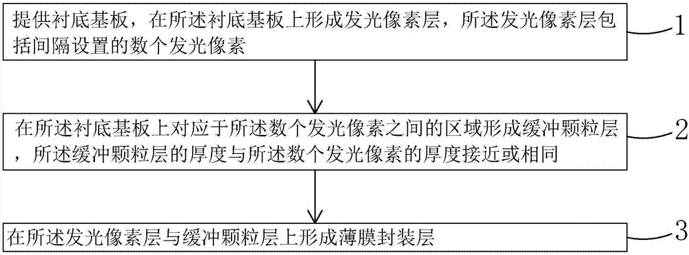
[0038] see figure 1 , the present invention provides a kind of OLED encapsulation method, comprises the following steps:

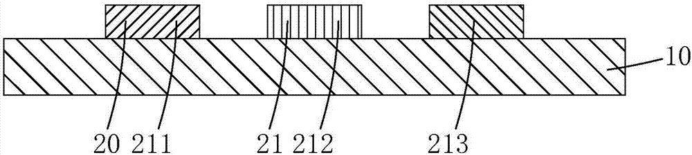
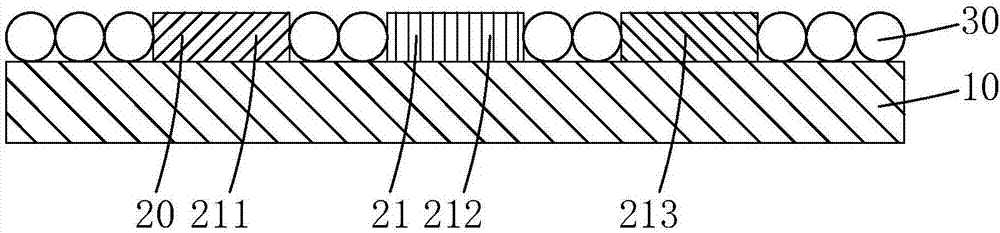
[0039] Step 1, such as figure 2 As shown, a base substrate 10 is provided, on which a light emitting pixel layer 20 is formed, and the light emitting pixel layer 20 includes several light emitting pixels 21 arranged at intervals.

[0040] Specifically, the thicknesses of the several light-emitting pixels 21 are close to or the same.

[0041] Specifically, the base substrate 10 is a flexible substrate, preferably a polyimide film.

[0042] Specifically, the plurality of light-emitting pixels 21 includes several red light-emitting pixels 211 , several green light-emitting pixels 212 and several blue light-emitting pixels...


PUM


Abstract

The invention provides an OLED packaging method and an OLED packaging structure. The OLED packaging method, by forming a buffer granular layer, realizes the planarization of a film packaging layer and reduces the fracture probability of the film packaging layer located at the edges of light-emitting pixels. The buffer granular layer can simultaneously resist water and oxygen so as to enhance the packaging effect of the prepared OLED packaging structure. The OLED packaging method, by forming the buffer granular layer, realizes the planarization of the film packaging layer and reduces the fracture probability of the film packaging layer located at the edges of light-emitting pixels, and has an excellent packaging effect.

Description

technical field [0001] The invention relates to the field of display technology, in particular to an OLED packaging method and an OLED packaging structure. Background technique [0002] Organic light-emitting diode (Organic Light-Emitting Diode, OLED) display, also known as organic electroluminescent display, is a new type of flat panel display device, due to its simple preparation process, low cost, low power consumption, high luminance, Wide range of working temperature, light and thin size, fast response speed, easy to realize color display and large-screen display, easy to realize matching with integrated circuit driver, easy to realize flexible display, etc., so it has broad application prospects. [0003] According to the driving method, OLED can be divided into two categories: passive matrix OLED (Passive Matrix OLED, PMOLED) and active matrix OLED (Active Matrix OLED, AMOLED), namely direct addressing and thin film transistor (TFT, Thin Film Transistor) There are tw...

Claims


Application Information

Patent Timeline
IPC IPC(8): H01L51/52H01L51/56
CPCH10K50/84H10K50/844H10K71/00
Inventor 黄辉
Owner TCL CHINA STAR OPTOELECTRONICS TECH CO LTD
Why Eureka
Try Eureka