
Fabrication method of super junction power device

A manufacturing method and technology for power devices, which are used in semiconductor/solid-state device manufacturing, semiconductor devices, electrical components, etc., can solve problems such as charge imbalance between P-type pillars and N-type epitaxial layers, reduce manufacturing costs, and improve withstand voltage. performance effect

Active Publication Date: 2020-03-06
FOUNDER MICROELECTRONICS INT
View PDF10 Cites 0 Cited by
  • Summary
  • Abstract
  • Description
  • Claims
  • Application Information

AI Technical Summary

Problems solved by technology

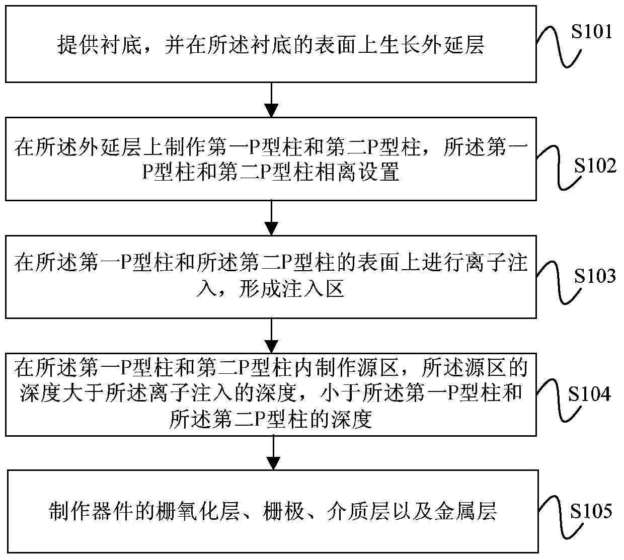
[0005] An embodiment of the present invention provides a method for manufacturing a super junction power device, which is used to solve the problem of charge imbalance between the P-type column and the N-type epitaxial layer caused by the high-temperature drive-in process in the traditional process

Method used


Image

  • Fabrication method of super junction power device
  • Fabrication method of super junction power device
  • Fabrication method of super junction power device

Examples


Embodiment Construction

[0026] The following will clearly and completely describe the technical solutions in the embodiments of the present invention with reference to the accompanying drawings in the embodiments of the present invention. Obviously, the described embodiments are only some, not all, embodiments of the present invention. Based on the embodiments of the present invention, all other embodiments obtained by persons of ordinary skill in the art without making creative efforts belong to the protection scope of the present invention.

[0027] The terms "comprising" and "having" and any variations thereof in the description and claims of the present invention are intended to cover a non-exclusive inclusion, for example, a process comprising a series of steps or a device of structure need not be limited to the expressly listed Instead, those structures or steps may include other steps or structures not expressly listed or inherent to the process or device.

[0028] figure 1 A schematic flow c...


PUM

PropertyMeasurementUnit
widthaaaaaaaaaa

Abstract

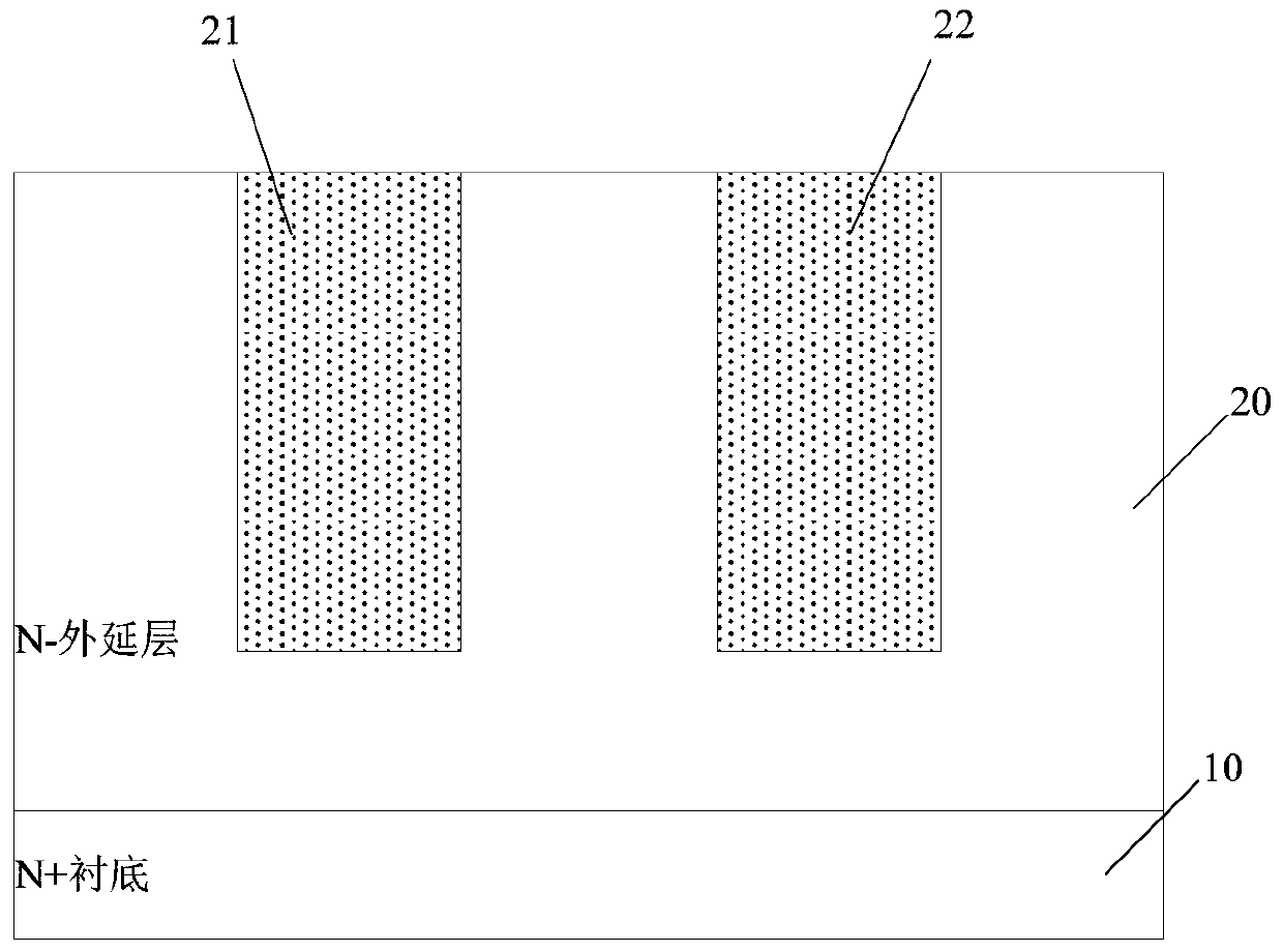
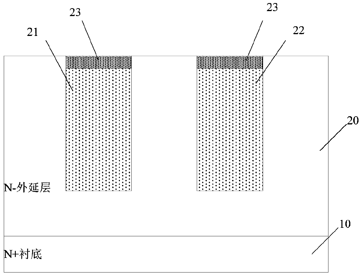
The embodiments of the present invention provide a fabrication method of a super-junction power device. The method includes the following steps that: a substrate is provided, and an epitaxial layer is grown on the surface of the substrate; a first P-type pillar and a second P-type pillar are fabricated on the epitaxial layer; ion implantation is performed on the surfaces of the first P-type pillar and the second P-type pillar, so that ion concentration on the surfaces of the first P-type pillar and the second P-type pillar can be decreased, and the depth of the ion implantation is smaller than the depth of the first P-type pillar and the second P-type pillar; source regions are fabricated in the first P-type pillar and the second P-type pillar, the depth of the source regions is greater than the depth of the ion implantation and is smaller than the depth of the first P-type pillar and the second P-type pillar; and the gate oxide layer, gate, dielectric layer and metal layer of the device are fabricated. With the method provided by the embodiments of the present invention adopted, the problem of charge imbalance between P-type pillars and an N-type epitaxial layer caused by a high-temperature drive-in process in a conventional process can be avoided, and the withstand voltage performance of the device can be improved.

Description

technical field [0001] Embodiments of the present invention relate to the technical field of semiconductors, and in particular to a method for manufacturing a super junction power device. Background technique [0002] In the prior art, the method of reducing the power loss by reducing the on-resistance of the semiconductor device is a common method in the semiconductor field. [0003] However, since the breakdown voltage of a semiconductor device is inversely proportional to the on-resistance, when the on-resistance decreases, the breakdown voltage of the device tends to be adversely affected. In order to solve this problem, a super junction power device has been introduced in the art, which includes alternating P-type regions and N-type regions located below the active region of the device. The alternating P-type regions and N-type regions in super-junction power devices are ideally in a state of charge balance, and these alternating P-type regions and N-type regions are m...

Claims


Application Information

Patent Timeline
Patent Type & Authority Patents(China)
IPC IPC(8): H01L21/336H01L29/78H01L29/06
CPCH01L29/0634H01L29/66477H01L29/78
Inventor 赵圣哲
Owner FOUNDER MICROELECTRONICS INT
Learn More