Method and apparatus for optimizing reverse recovery characteristic of body diode

A technology of reverse recovery and body diode, which is applied in semiconductor devices, semiconductor/solid-state device manufacturing, electrical components, etc., can solve the problems of false gate opening, high voltage change rate of reverse recovery characteristics, high power consumption of devices, etc., to achieve Reduce the reverse voltage conversion rate, optimize the reverse recovery characteristics, and improve the effect of softness

Inactive Publication Date: 2017-11-17
苏州达晶微电子有限公司
View PDF4 Cites 3 Cited by
  • Summary
  • Abstract
  • Description
  • Claims
  • Application Information

AI Technical Summary

Problems solved by technology

The poor reverse recovery characteristics of the body diode will produce a very high voltage change rate (dv / dt), which may cause many problems such as excessive power consumption of the device during reverse recovery and the occurrence of false gate turn-on, so the body diode The reverse recovery characteristics of the device are extremely critical factors affecting the application reliability of the device

Method used


Image

  • Method and apparatus for optimizing reverse recovery characteristic of body diode
  • Method and apparatus for optimizing reverse recovery characteristic of body diode
  • Method and apparatus for optimizing reverse recovery characteristic of body diode

Examples


Embodiment

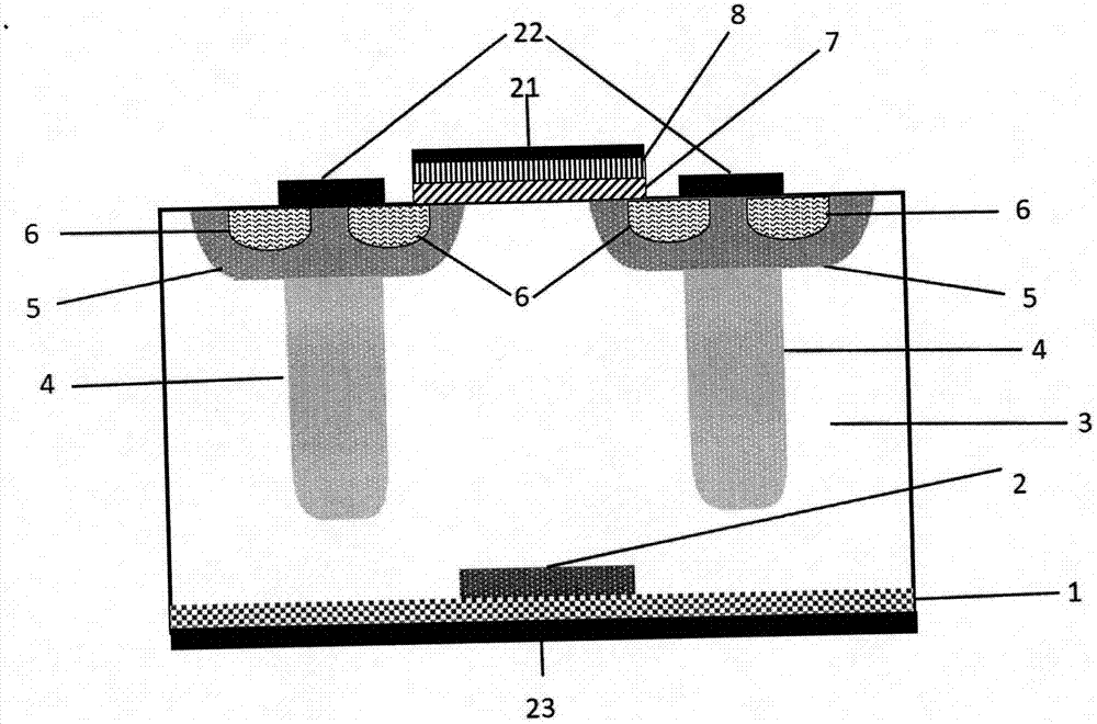
[0039] 1. Substrate material preparation, using an n-type zone-fused monocrystalline silicon substrate 3 with a resistivity of 21 Ω·cm and a thickness of 725 μm, and its crystal orientation is ;

[0040] 2. Make a COOLMOS device structure on an n-doped substrate, including p-column 4, p+ doped region 5, n+ doped region 6, gate oxide layer 7, gate polysilicon 8, gate metal electrode 21, source metal electrodes 22;

[0041] 3. Use a thinning machine to thin the wafer to 60 μm. like figure 2 shown.

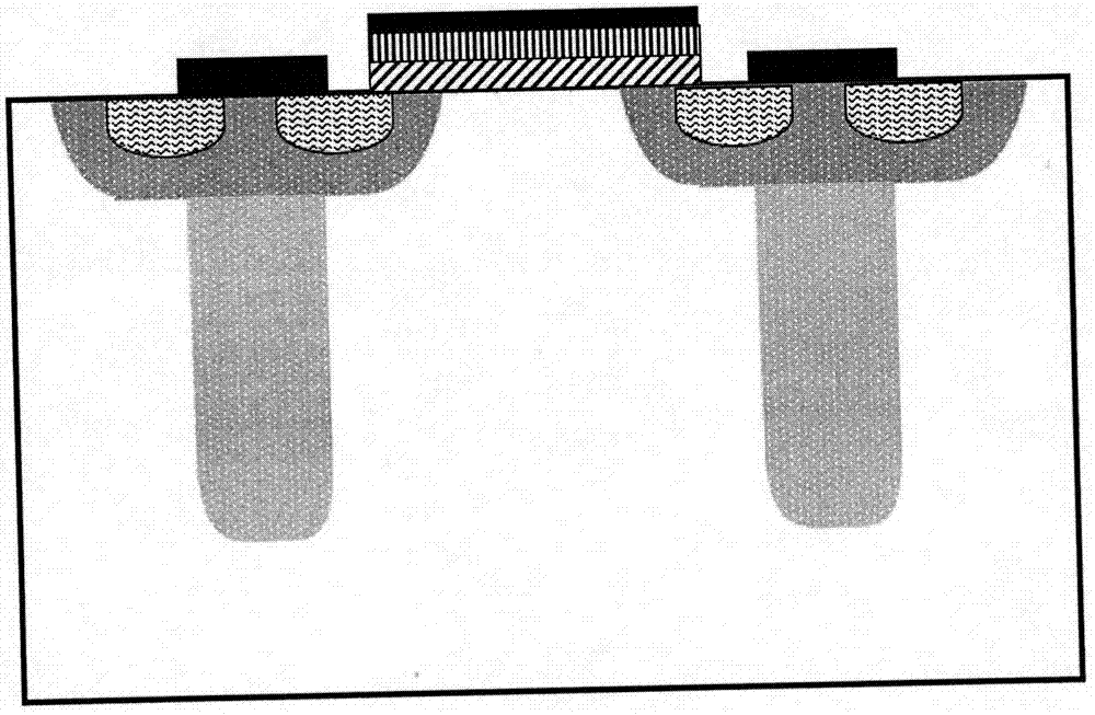
[0042] 4. Use n heavily doped photolithography mask to expose the back of the thinned n-doped substrate, and use photoresist to block local n-type ion implantation with an implantation dose of 1e 14 cm -2 , the implantation energy is 1000kev, and the implantation depth is about 1μm, such as image 3 shown.

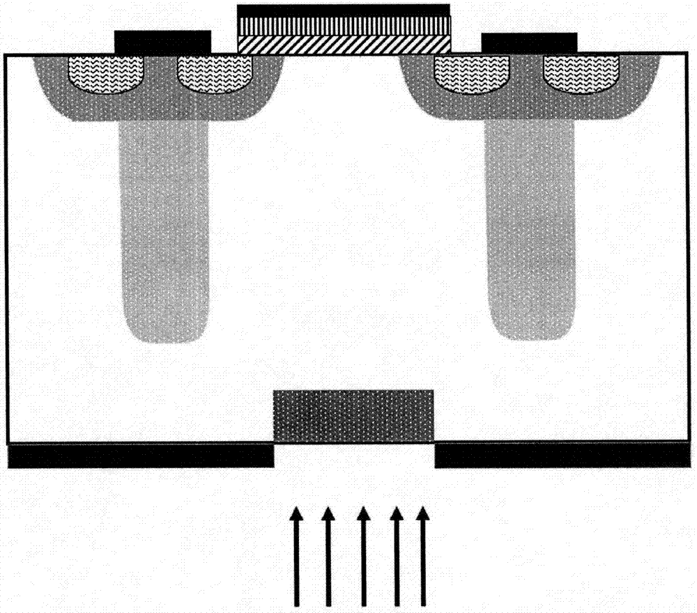
[0043] 5. Remove the photoresist in step 4, and implant global n-type super-heavily doped ions on the back of the device, with an implantation dose of 3e 15 cm -2 , the ...


PUM


Abstract

The invention discloses a method and an apparatus for optimizing reverse recovery characteristic of a body diode. Processing is preformed for a COOLMOS device, wherein a drain region is formed at the bottom of the COOLMOS device; and the doping concentration of an n heavily doped region is higher than that of an n doped substrate region. By forming the n type heavy doping to partial regions on the back surface of the device after the device is thinned, a partial buffer layer structure can be formed, so that the reverse recovery softness of the body diode is improved and reverse voltage conversion rate (dv/dt) is lowered, thereby optimizing the reverse recovery characteristic of the body diode.

Description

technical field [0001] The invention relates to a method and a device for optimizing the reverse recovery characteristic of a body diode. Background technique [0002] In high-voltage switching applications, it is necessary to use high-voltage MOS devices with good body diodes and strong durability, but the high on-resistance of conventional high-voltage MOS devices increases the static power consumption of switching circuits. With the increase of super-junction devices With the development, many manufacturers have developed COOLMOS devices made of different process technologies. Compared with ordinary high-voltage MOS devices, COOLMOS devices have lower conduction internal resistance, so they can have lower operating losses. It has been widely used in many industries. [0003] An ordinary pn junction body diode is parasitic in the conventional COOLMOS structure. The switching process of the diode from the on state to the reverse blocking state is called reverse recovery. ...

Claims


Application Information

Patent Timeline
Patent Type & Authority Applications(China)
IPC IPC(8): H01L21/336H01L29/08H01L29/78
CPCH01L29/0847H01L29/66666H01L29/7827
Inventor 不公告发明人
Owner 苏州达晶微电子有限公司
Why Eureka
Try Eureka