A method and device for realizing BGA chip rework by using laser

A chip and laser technology, applied in the direction of semiconductor devices, electrical components, circuits, etc., can solve the problems of large heat-affected range, long alignment time, and difficult BGA chip repair, so as to achieve simple structure and/or principle and avoid disadvantages The effect of affecting and shortening the repair time

Active Publication Date: 2020-09-11
HUBEI SANJIANG AEROSPACE HONGFENG CONTROL
View PDF9 Cites 0 Cited by
  • Summary
  • Abstract
  • Description
  • Claims
  • Application Information

AI Technical Summary

Problems solved by technology

[0003] As the integration level of the chip is getting higher and higher, the number of I / O leads is also increasing. On the basis of ensuring the miniaturization of the chip, the pin pitch of the chip is getting smaller and smaller. Grid array package chip) and CSP chip (Chip Scale Package, chip size package) are particularly obvious. The advent and development of chips such as BGA chips and CSP chips have greatly promoted the miniaturization and intelligence of electronic products. However, due to The pin spacing of the BGA chip is very small, and the PCB board on which the BGA chip is installed is usually installed with other electronic components at a high density. Therefore, it is difficult to repair the BGA chip. craft to complete
[0004] In the existing BGA chip rework field, a BGA rework station based on infrared heating is usually used, such as a BGA intelligent rework station disclosed in the patent document CN 201520222667.6, which includes an operating table, an infrared heating device, a control device and a display device , the infrared heating device is connected to the operating table, and the control device and the display device are connected through a diode circuit. In this scheme, the infrared heating device is used to heat and desolder the BGA chip, although it can realize the overhaul of the BGA chip more accurately and positioning; however, the above-mentioned type of BGA chip rework station also has great limitations, for example: 1. The infrared heating device has a large heat-affected range, which is easy to affect the components around the BGA chip. Components are soldered or desoldered; 2. The existing infrared-based heating device and the BGA chip take a long time to align, and the alignment accuracy is poor, which greatly reduces the repair efficiency of the BGA chip. Although there are BGA repair A CCD imaging system is installed on the stage to achieve optical alignment to improve the alignment accuracy between the heating device and the BGA chip. However, after the size of the PCB board is changed, it is necessary to manually adjust the position of the PCB board many times to achieve the optical alignment between the BGA chip and the imaging system. bit, greatly reducing the efficiency of BGA chip rework
Therefore, the existence of the above-mentioned defects greatly affects the accuracy and efficiency of the repair of existing BGA chips, which has a great adverse effect on the application and development of BGA chips, and indirectly affects the miniaturization and intelligent development of electronic products. Increased application and maintenance costs of BGA chips

Method used


Image

  • A method and device for realizing BGA chip rework by using laser
  • A method and device for realizing BGA chip rework by using laser

Examples


Embodiment Construction

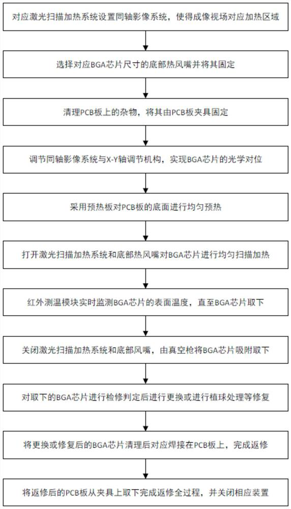
[0040] In order to make the object, technical solution and advantages of the present invention clearer, the present invention will be further described in detail below in conjunction with the accompanying drawings and embodiments. It should be understood that the specific embodiments described here are only used to explain the present invention, not to limit the present invention.

[0041] In addition, the technical features involved in the various embodiments of the present invention described below can be combined with each other as long as they do not constitute a conflict with each other.

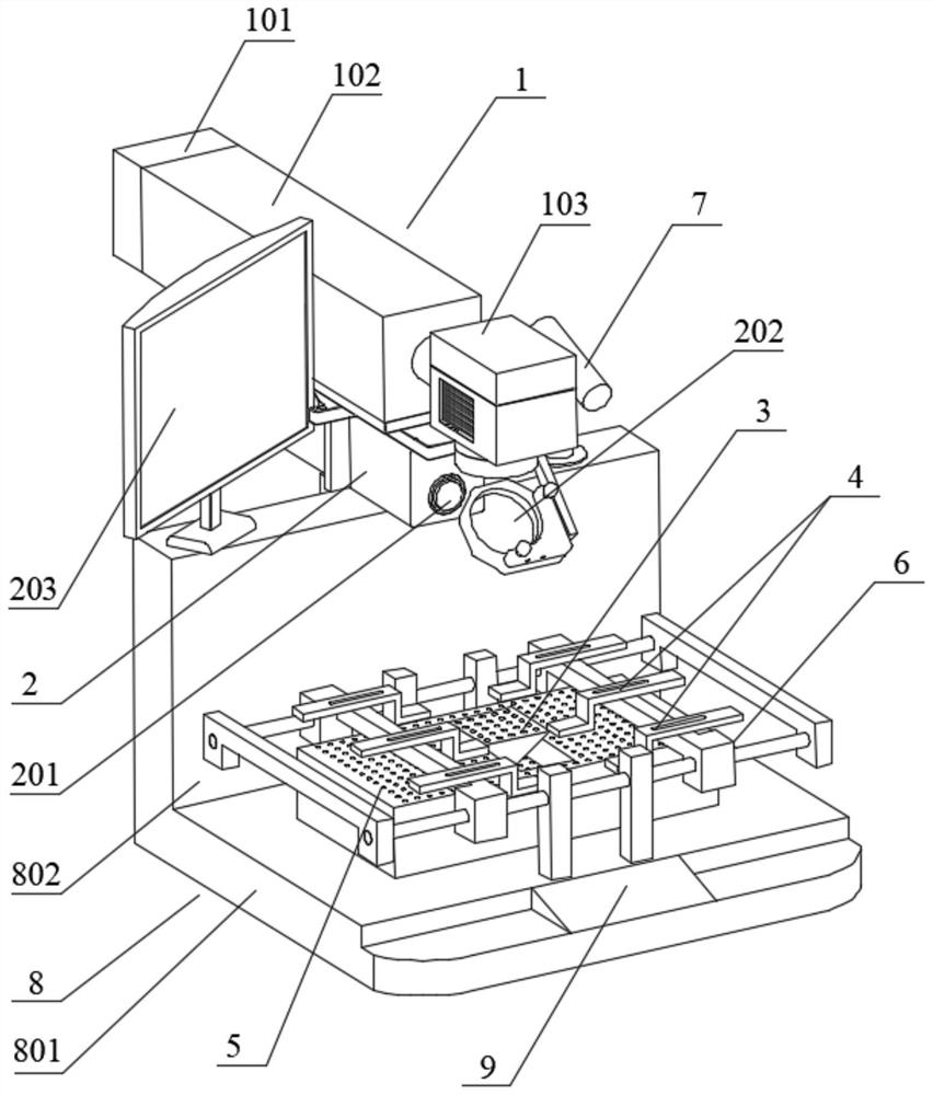
[0042] Specifically, such as figure 2 Shown is a schematic structural diagram of a device for using laser to realize BGA chip rework in a preferred embodiment of the present invention, which includes a laser scanning heating system 1, a coaxial imaging system 2, a bottom hot air nozzle 3, a PCB board fixture 4, and a preheating plate 5 , X-Y axis adjustment mechanism 6, infrared tempe...


PUM


Abstract

The present invention disclose a method and a device capable of realizing repair of a BGA chip by using lasers, pertaining to the field of printed circuit board manufacturing. The device comprises a laser scanning heating system, a coaxial imaging system, a bottom hot-air nozzle, a pre-heating board and a PCB board fixture. According to the device, by performing a coaxial arrangement on a laser beam axis of the laser scanning heating system and a visible light reflection axis of the coaxial imaging system, and by allowing an irradiation area of laser beams to face the bottom hot-air nozzle, corresponding setting of the coaxial imaging system, the laser scanning heating system and the bottom hot-air nozzle is realized, and thus alignment of the BGA chip, the bottom hot-air nozzle and a laser scanning heating head can be realized with the only requirement of adjustment of a visual field position of the BGA chip on the coaxial imaging system. According to the method and the device, the effect on the other components around is effectively reduced in the repair process of the BGA chip, the alignment time of the BGA chip is greatly shortened in the repair process, the repair efficiency of the BGA chip is greatly improved, and the application cost of the BGA chip is reduced.

Description

technical field [0001] The invention belongs to the field of printed circuit board manufacturing, and in particular relates to a method and a device for realizing BGA chip repair by using laser. Background technique [0002] With the continuous development of electronic technology, electronic products tend to be more miniaturized, portable and intelligent, and the traditional line connection form has also undergone major changes. Printed circuit boards (also known as printed circuit boards, referred to as PCB boards) The application has become more and more extensive. Correspondingly, various chips corresponding to the PCB board have also been rapidly developed, and have been widely used in various electronic products. [0003] As the integration level of the chip is getting higher and higher, the number of I / O leads is also increasing. On the basis of ensuring the miniaturization of the chip, the pin pitch of the chip is getting smaller and smaller. Grid array package chip...

Claims


Application Information

Patent Timeline
Patent Type & Authority Patents(China)
IPC IPC(8): H01L21/67
CPCH01L21/67H01L21/67115H01L2221/67
Inventor 张庸周鹏
Owner HUBEI SANJIANG AEROSPACE HONGFENG CONTROL
Why Eureka
Try Eureka