Epitaxial wafer of light-emitting diode and preparation method thereof

A technology of light-emitting diodes and epitaxial wafers, which is applied in the field of optoelectronics and can solve problems such as large warpage of epitaxial wafers.

Active Publication Date: 2017-11-17
HC SEMITEK CORP
View PDF5 Cites 2 Cited by
  • Summary
  • Abstract
  • Description
  • Claims
  • Application Information

AI Technical Summary

Problems solved by technology

[0005] In order to solve the problem of large warpage of the epitaxial wafer in the existing GaN-based LED, an embodiment of the present invention provides an epitaxial wafer of a light-emitting diode and a preparation method thereof

Method used


Image

  • Epitaxial wafer of light-emitting diode and preparation method thereof
  • Epitaxial wafer of light-emitting diode and preparation method thereof
  • Epitaxial wafer of light-emitting diode and preparation method thereof

Examples


Embodiment Construction

[0024] In order to make the object, technical solution and advantages of the present invention clearer, the implementation manner of the present invention will be further described in detail below in conjunction with the accompanying drawings.

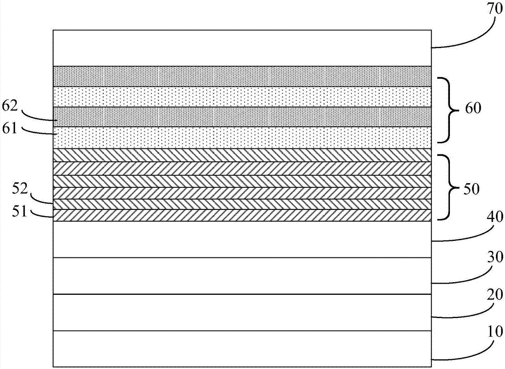
[0025] figure 1 It is a schematic structural diagram of an epitaxial wafer of a light emitting diode provided by an embodiment of the present invention, as shown in figure 1 As shown, the epitaxial wafer includes a substrate 10 and a buffer layer 20, a u-type GaN layer 30, an n-type GaN layer 40, a stress release layer 50, an active layer 60 and a p-type GaN layer 70 stacked on the substrate 10 in sequence. , wherein the stress release layer 50 includes multiple layers of In alternately stacked x Ga (1-x) N layer 51 and multilayer n-type Al y Ga (1-y) N layer 52, and multiple layers of In x Ga (1-x) The composition content of In in the N layer 51 increases layer by layer, and the active layer 60 includes multiple layers of In alt...


PUM


Abstract

The invention discloses an epitaxial wafer of a light-emitting diode and a preparation method thereof and belongs to the technical field of phoelectrons. The epitaxial wafer includes a substrate, a buffer layer, a u-shaped GaN layer, an n-shaped GaN layer, a stress release layer, an active layer and a p-shaped GaN layer. The stress release layer includes InxGa (1-x) N alyers and n-shaped AlyGa (1-y) N layers which are alternated. Since the constituent component of In in the InxGa (1-x) N layers which approach the n-shaped GaN layer is smaller than the constituent component of In in the InxGa (1-x) N layers which approach the active layer, the stress release layer reduces the recession of the epitaxial wafer and has smaller protrusion. The constituent component of In in the InmGa (1-m) N well layer is smaller than the constituent component in the InxGa (1-x) N layer. The active layer makes the epitaxial layer to recess towards one side of the substrate when the active layer grows, which offsets the protrusion which is formed upon growing the stress release layer and reduces warpage of the epitaxial wafer.

Description

technical field [0001] The invention relates to the field of optoelectronic technology, in particular to an epitaxial wafer of a light emitting diode and a preparation method thereof. Background technique [0002] Light Emitting Diode (English: Light Emitting Diode, referred to as: LED), as a very influential new product in the optoelectronics industry, has the characteristics of small size, long service life, colorful colors, and low energy consumption. It is widely used in lighting, display screens , signal lights, backlight, toys and other fields. The core structure of the LED is the epitaxial wafer, and the production of the epitaxial wafer has a great influence on the photoelectric characteristics of the LED. [0003] Epitaxial wafers of GaN-based LEDs generally include a sapphire substrate and a buffer layer, u-type GaN layer, n-type GaN layer, active layer and p-type GaN layer stacked on the sapphire substrate in sequence. [0004] In the GaN-based LED epitaxial waf...

Claims


Application Information

Patent Timeline
Patent Type & Authority Applications(China)
IPC IPC(8): H01L33/12H01L33/14H01L33/00
CPCH01L33/007H01L33/12H01L33/145
Inventor 武艳萍
Owner HC SEMITEK CORP
Why Eureka
Try Eureka