Photoresist patterning method, preparation method of semiconductor structure, and semiconductor equipment
A patterning and photoresist technology is used in the preparation of semiconductor structures, photoresist patterning methods, and semiconductor equipment fields. The effect of production efficiency
- Summary
- Abstract
- Description
- Claims
- Application Information
AI Technical Summary
Problems solved by technology
Method used
Image


Examples
Embodiment 1
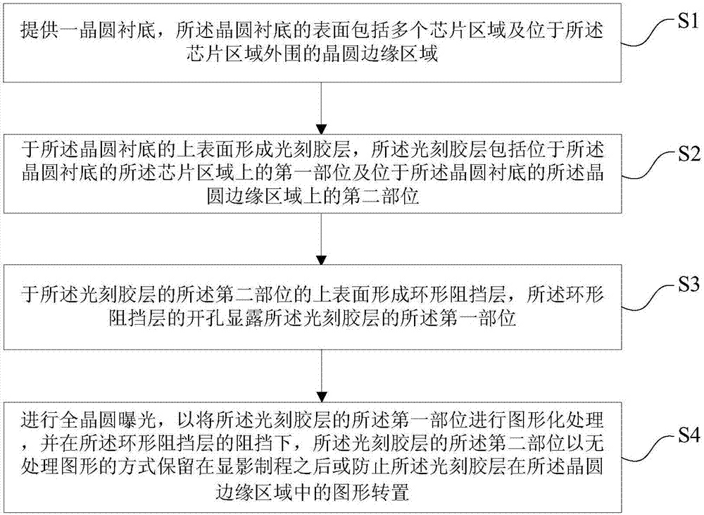
[0069] see figure 1 , the present invention provides a kind of photoresist patterning method, described photoresist patterning method comprises the following steps:
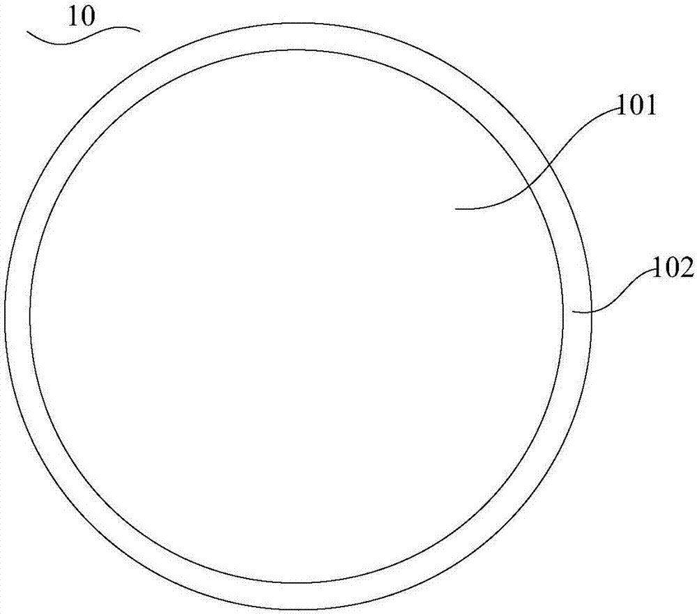
[0070] 1) providing a wafer substrate, the surface of the wafer substrate includes a plurality of chip regions and a wafer edge region located at the periphery of the chip regions;
[0071] 2) forming a photoresist layer on the upper surface of the wafer substrate, the photoresist layer including a first portion located on the chip region of the wafer substrate and a first portion located on the wafer substrate a second location on the edge region of the wafer;
[0072] 3) forming an annular barrier layer on the upper surface of the second portion of the photoresist layer, the opening of the annular barrier layer revealing the first portion of the photoresist layer;
[0073] 4) performing full-wafer exposure to pattern the first part of the photoresist layer, and under the barrier of the annular barrier layer, ...
Embodiment 2
[0096] see Figure 9 , the present invention also provides a method for preparing a semiconductor structure, the method for preparing a semiconductor structure includes the following steps:
[0097] 1) providing a wafer substrate, the surface of the wafer substrate includes a plurality of chip areas and a wafer edge area located at the periphery of the chip areas;
[0098] 2) forming a hard mask layer on the upper surface of the wafer substrate;
[0099] 3) forming a photoresist layer on the upper surface of the hard mask layer, the photoresist layer including the first part on the chip area of the wafer substrate and the first part located on the wafer substrate a second location on the edge region of the wafer;
[0100] 4) forming an annular barrier layer on the upper surface of the second portion of the photoresist layer, the opening of the annular barrier layer revealing the first portion of the photoresist layer;
[0101] 5) performing full-wafer exposure to pattern ...
Embodiment 3
[0143] see Figure 20 , the present invention also provides a photoresist coating equipment, the photoresist coating equipment is used to implement step 2) to step 3) in the first embodiment, or to implement the step 3) to step 3) in the second embodiment Step 4), the photoresist coating equipment includes: a wafer carrier 20, the wafer carrier 20 is suitable for placing the wafer substrate 10, and drives the wafer substrate 10 to rotate; Spraying system, the photoresist spraying system includes a photoresist supply source (not shown), a first supply pipeline (not shown) and a photoresist nozzle 21; wherein, one end of the first supply pipeline is connected to The photoresist supply source is connected; the photoresist nozzle 21 is located above the center of the wafer carrier 20 (that is, when the wafer substrate 10 is located on the wafer carrier 20, the The photoresist nozzle 21 is directly facing the center of the wafer substrate 10), and communicates with the end of the ...
PUM
| Property | Measurement | Unit |
|---|---|---|
| width | aaaaa | aaaaa |
Abstract
Description
Claims
Application Information
PatSnap Eureka turns technology decisions into work you can execute. Powered by our Innovation Knowledge Graph, it runs expert workflows across engineering, life sciences, materials and intellectual property. Get your review-ready output in minutes.


