Production method of thin film transistor

A technology of thin-film transistors and manufacturing methods, which is applied in the direction of transistors, semiconductor/solid-state device manufacturing, semiconductor devices, etc., and can solve the problems that the amorphous silicon TFT process cannot be completely replicated.

Inactive Publication Date: 2017-11-21
NANJING CEC PANDA FPD TECH CO LTD +2
View PDF4 Cites 9 Cited by
  • Summary
  • Abstract
  • Description
  • Claims
  • Application Information

AI Technical Summary

Problems solved by technology

Therefore, the process parameters and process conditions of IGZO TFT will not be exactly the same as those of amorphous silicon TFT. That is to

Method used


Image

  • Production method of thin film transistor
  • Production method of thin film transistor
  • Production method of thin film transistor

Examples


Embodiment Construction

[0030] Below in conjunction with accompanying drawing and specific embodiment, further illustrate the present invention, should be understood that these embodiments are only for illustrating the present invention and are not intended to limit the scope of the present invention, after having read the present invention, those skilled in the art will understand various aspects of the present invention Modifications in equivalent forms all fall within the scope defined by the appended claims of this application.

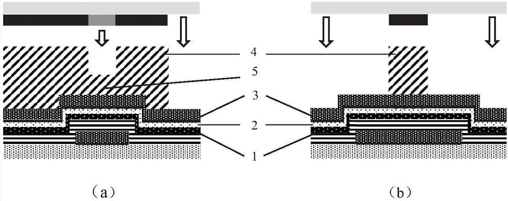
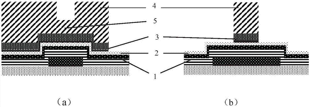
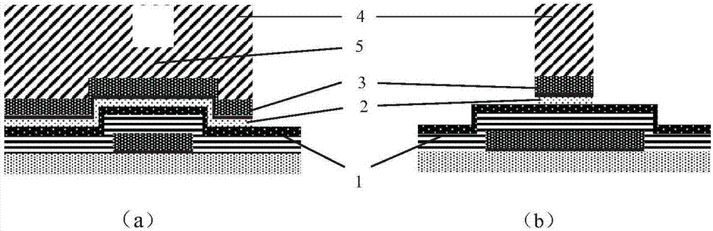
[0031] Figure 1-Figure 6 It is a schematic diagram of the steps of the manufacturing method of the thin film transistor of the present invention, wherein (a) is a pixel part / GDM part, and (b) is a terminal part.

[0032] The manufacturing method of thin film transistor of the present invention comprises:

[0033] In the first step, the semiconductor layer 2 and the source-drain metal layer 3 are deposited in sequence.

[0034] In the second step, a photoresist layer 4 ...


PUM


Abstract

The invention provides a production method of a thin film transistor. The method comprises the following steps of sequentially depositing a semiconductor layer and a metal layer; coating a photoresist layer on the metal layer; exposing the photoresist layer, patterning the photoresist layer, wherein one part of the photoresist layer is formed into a thin photoresist layer, and the other part is formed into the thick photoresist layer or non-photoresist layer; etching primarily: etching the metal layer and the semiconductor layer to remove the part covered by the non-photoresist layer; graying the photoresist layer, and removing the thin photoresist layer to expose the metal layer positioned under the thin photoresist layer; etching secondarily: etching the metal layer to form a source, a drain and a channel area and expose the semiconductor layer positioned in the channel area; and removing the photoresist layer. According to the production method provided by the invention, one time of utilization of a photomask is reduced, production cost of the thin film transistor is reduced, and a technological process is optimized.

Description

technical field [0001] The invention belongs to the technical field of thin film transistors, and in particular relates to a manufacturing method of thin film transistors. Background technique [0002] Among flat panel display devices, Thin Film Transistor Liquid Crystal Display (TFT-LCD for short) has the characteristics of small size, low power consumption, relatively low manufacturing cost and low radiation. [0003] In order to form a TFT (Thin Film Transistor, thin film transistor) array on a transparent substrate, in the TFT array production process, it is necessary to use a certain number of photomasks (Photo Mask) to repeatedly perform film formation, exposure, and etching on the substrate. and other photolithography processes to form the leads, electrodes, terminals, and insulating film layers of the TFT array. Since the mass production of TFT-LCD began in 1993, in order to reduce production costs and improve product yield, various manufacturers have continuously c...

Claims


Application Information

Patent Timeline
IPC IPC(8): H01L29/786H01L21/336
CPCH01L29/66969H01L29/7869
Inventor 郝光叶简锦诚戴超周刘飞王志军
Owner NANJING CEC PANDA FPD TECH CO LTD
Why Eureka
Try Eureka