Power semiconductor device structure suitable for deep groove and manufacturing method

A power semiconductor and device structure technology, applied in semiconductor/solid-state device manufacturing, semiconductor devices, electrical components, etc., can solve problems such as increased difficulty, achieve the effects of suppressing electric field concentration, reducing curvature, and enhancing horizontal depletion

Active Publication Date: 2017-11-28
WUXI NCE POWER
View PDF3 Cites 8 Cited by
  • Summary
  • Abstract
  • Description
  • Claims
  • Application Information

AI Technical Summary

Problems solved by technology

Therefore, the terminal design of deep trench devices is more difficult than that of general power devices

Method used


Image

  • Power semiconductor device structure suitable for deep groove and manufacturing method
  • Power semiconductor device structure suitable for deep groove and manufacturing method
  • Power semiconductor device structure suitable for deep groove and manufacturing method

Examples


Embodiment Construction

[0042] The present invention will be further described below in conjunction with specific drawings and embodiments.

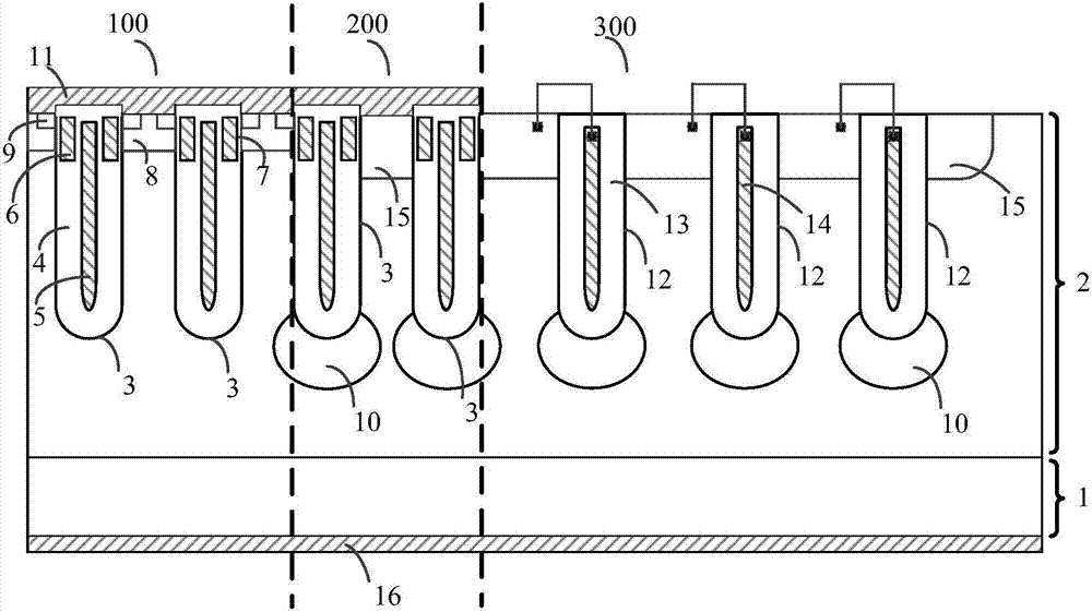
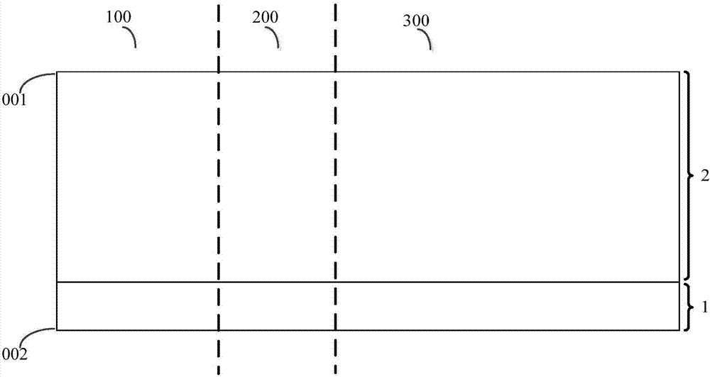
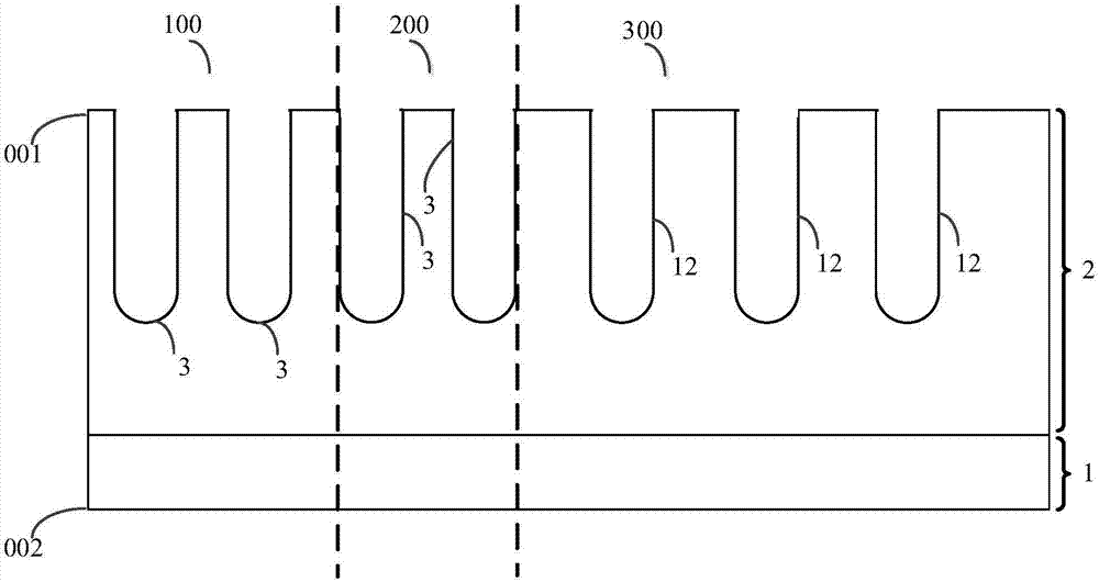
[0043] Such as figure 1 As shown, in order to effectively improve the high-voltage resistance characteristics of the device, reduce the cost, and improve the scope of application, the present invention proposes a semiconductor structure and a manufacturing method suitable for deep trench devices. In the semiconductor device of N-type deep trench MOSFET Taking a shielded gate power MOSFET as an example, on the top view plane of the semiconductor device, it includes an active region 100, a terminal transition region 200 and a terminal protection region 300 located on the semiconductor substrate, and the active region 100 is located at the center of the semiconductor substrate area, the terminal transition area 200 is located at the outer circle of the active area 100 and surrounds the active area 100, and the terminal protection area 300 is located at the outer c...


PUM


Abstract

The invention relates to a power semiconductor device structure suitable for a deep groove and a manufacturing method. The power semiconductor device structure is characterized in that on the cross section of a semiconductor device, a second conductive type of a second well region is arranged on the surface of a first conductive type of a drift region of a terminal protection region; a plurality of a second type of grooves are formed in the second conductive type of the second well region; central regions in the second type of the grooves are filled with a second type of conductors and a second type of dielectric bodies located on the outer circles of the second type of the conductors; the second type of the conductors are electrically connected with the second conductive type of the second well region close to one side of a terminal transitional region outside the second type of the grooves in which the second type of the conductors are located; and a second conductive type of third well regions are arranged below a first type of grooves in the terminal transitional region and the second type of the grooves in the terminal protection region. According to the structure, the high voltage resistance of the device can be effectively improved; a manufacturing process is compatible with an existing semiconductor process; the application range is wide; and the production cost is reduced.

Description

technical field [0001] The invention relates to a power semiconductor device and a manufacturing method, in particular to a power semiconductor device suitable for deep trenches and a manufacturing method, and belongs to the technical field of manufacturing semiconductor devices. Background technique [0002] Regulatory agencies and end customers are increasingly demanding DC-DC power supply efficiency, and new designs of power semiconductor devices require lower on-resistance without compromising unclamped inductive switching (UIS) capability or increasing switching losses . [0003] DC-DC power supply designers are always faced with the challenge of improving efficiency and power density. On-resistance (Rds-on) and gate charge (Qg) are two key parameters of power semiconductor devices. Generally, one is always reduced and the other is reduced. One increases, so power MOSFET designers must consider the trade-off between the two, and the continuous advancement of power MOSF...

Claims


Application Information

Patent Timeline
Patent Type & Authority Applications(China)
IPC IPC(8): H01L29/78H01L29/06H01L21/336
CPCH01L29/0607H01L29/0684H01L29/66666H01L29/7827Y02B70/10
Inventor 朱袁正叶鹏周锦程
Owner WUXI NCE POWER
Why Eureka
Try Eureka