High-throughput FFT/IFFT-based FPGA signal processing method
A high throughput and signal processing technology, applied in the field of FPGA technology, can solve the problems of consuming hardware resources, less DFT transformation throughput, etc., and achieve the effects of reducing hardware consumption, easy engineering implementation, and reducing parallelism
- Summary
- Abstract
- Description
- Claims
- Application Information
AI Technical Summary
Problems solved by technology
Method used
Image
Examples
Embodiment 1
[0021] This embodiment only illustrates the steps of writing / reading / outputting the RAM.
[0022] The RAM storage area reading and writing mode of the present invention refers to Figure 4 , the RAM is regarded as a circular arrangement of multiple storage areas, and each storage area is sequentially numbered 1, 2, 3... in a clockwise direction. Figure 4 is a simplified schematic diagram containing 32 memory areas. First read the data from the 30MHz low-frequency signal, and write the read data content to the storage area sequentially and cyclically in the order of the storage area, that is, after the storage area with the serial number 32 is written, the storage area with the serial number 1 As a continuation, a loop is formed. The read clock is high frequency, such as 150MHz higher than 30MHz, and the data is read from the RAM in the form of a sliding window. Figure 4 The length of the middle sliding window is 8 storage areas, and the sliding step is 1 storage area.
...
Embodiment 2
[0029] Assuming that the input signal with a rate of 30MHz is x(n)n=0,1,2,..., a vector with a length of 64 at every other sampling point needs to perform a 64-point FFT operation, that is, the vector [x(0)x (1)...x(63)] needs to perform a 64-point FFT, and the vector [x(1)x(2)...x(64)] needs to perform a 64-point FFT, and the vector [x(2)x(3)... x(65)] requires a 64-point FFT.
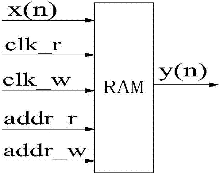
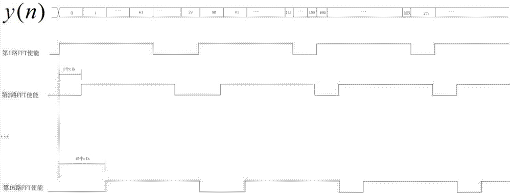
[0030] To the FPGA realization of the above-mentioned problem, the present invention adopts the mode that data rate multiplication and parallel processing combine to calculate, and its realization block diagram is as follows Figure 1 to Figure 3 as shown, figure 1 Indicates that the 30MHz signal is converted into a 150MHz signal, and the signal rate is increased by 5 times, so that subsequent modules can operate at a higher frequency; figure 2 Indicates the rate conversion control diagram, which controls the input and output signal addresses, image 3 It means that the above calculation is realiz...
PUM
 Abstract
Description
Claims
Application Information


