Method For Producing Semiconductor Epitaxial Wafer, Semiconductor Epitaxial Wafer, And Method For Manufacturing Solid-State Imaging Element

A manufacturing method, epitaxial wafer technology, applied in semiconductor/solid-state device manufacturing, semiconductor devices, electric solid-state devices, etc., can solve problems such as insufficient, heavy metal pollution of semiconductor substrates, etc., and achieve the effect of high gettering capacity

Active Publication Date: 2017-12-08
SUMCO CORP
View PDF9 Cites 0 Cited by
  • Summary
  • Abstract
  • Description
  • Claims
  • Application Information

AI Technical Summary

Problems solved by technology

In recent years, these metal contaminations have been improved to some extent by replacing the constituent materials of the epitaxial growth furnace with materials with excellent corrosion resistance, etc., but not sufficiently.
On the other hand, in the latter, that is, in the manufacturing process of solid-state imaging devices, heavy metal contamination of semiconductor substrates is also a concern in various processes such as ion implantation, diffusion, and oxidation heat treatment.

Method used


Image

  • Method For Producing Semiconductor Epitaxial Wafer, Semiconductor Epitaxial Wafer, And Method For Manufacturing Solid-State Imaging Element
  • Method For Producing Semiconductor Epitaxial Wafer, Semiconductor Epitaxial Wafer, And Method For Manufacturing Solid-State Imaging Element
  • Method For Producing Semiconductor Epitaxial Wafer, Semiconductor Epitaxial Wafer, And Method For Manufacturing Solid-State Imaging Element

Examples


experiment example 2

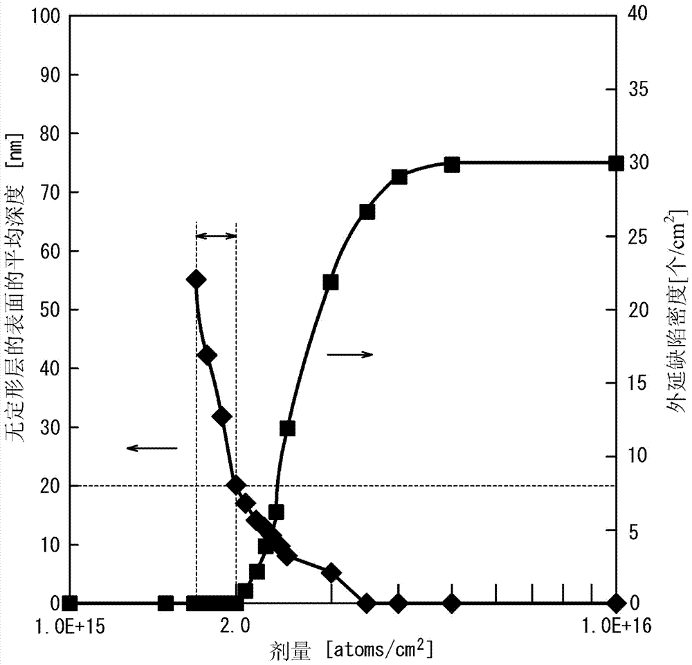
[0098] In addition to carbon dosing such as image 3 As shown in the graph, from 1.0 x 10 15 atoms / cm 2 to 1.0×10 16 atoms / cm 2 Except for the multiple conditions, the same method as in Experimental Example 1 was used to fabricate multiple silicon epitaxial wafers with different dosages.

[0099] The cross section around the modified layer after cluster ion irradiation was observed using TEM. Whether or not an amorphous layer was formed in the modified layer was measured, and when an amorphous layer was formed, the average depth of the surface of the amorphous layer on the semiconductor wafer surface side and the average thickness of the amorphous layer were measured. As a representative example of TEM image, the dose is 1.0×10 15 atoms / cm 2 The situation is shown in Figure 6 (A), the dose is 1.7×10 15 atoms / cm 2 The situation is shown in Figure 6 (B), the dose is 2.0×10 15 atoms / cm 2 The situation is shown in Figure 6 (C), the dose is 3.0×10 15 atoms / cm 2 Th...

experiment example 3

[0107] Except that the species of cluster ion is C generated from cyclohexane 3 h 3 Except clusters, the same experiment as in Experimental Example 2 was carried out to obtain Figure 4 the result of. It can be seen that in this case, it is possible to use 2.2×10 15 atoms / cm 2 The above dosage forms an amorphous layer and obtains high gettering capacity. On the other hand, it is possible to 15 atoms / cm 2 The following doses make the average depth 20 nm or more, thereby sufficiently suppressing the generation of epitaxial defects.

[0108] Also, at a dose of 2.2×10 15 atoms / cm 2 Above and 2.6×10 15 atoms / cm 2 In the range below, black dot-like defects were observed after the epitaxial layer was formed. At doses less than 2.2 x 10 15 atoms / cm 2 In the case of , black dot-like defects were not observed. At doses greater than 2.6 x 10 15 atoms / cm 2 In the case of , black dot-like defects were not observed, but a linear defect layer formed by connecting black dots wa...


PUM


Abstract

This method for producing a semiconductor epitaxial wafer (100) is characterized by comprising: a first step wherein a surface (10A) of a semiconductor wafer (10) is irradiated with cluster ions (12) so that a modified layer (14), in which the constituent element of the cluster ions is solid-solved, is formed in a surface portion of the semiconductor wafer; and a second step wherein an epitaxial layer (18) is formed on the modified layer (14) of the semiconductor wafer. This method for producing a semiconductor epitaxial wafer (100) is also characterized in that the first step is carried out so that a part of the modified layer (14) in the thickness direction forms an amorphous layer (16) and the average depth of the semiconductor wafer surface-side surface (16A) of the amorphous layer (16) is 20 nm or more from the semiconductor wafer surface (10A).

Description

[0001] The application date is December 10, 2014, the national application number is 201480068832.5 (the international application number is PCT / JP2014 / 083315), and the title of the invention is "Manufacturing method of semiconductor epitaxial wafer, semiconductor epitaxial wafer, and solid-state imaging device The divisional application of the application for the manufacturing method of ". technical field [0002] The present invention relates to a method for manufacturing a semiconductor epitaxial wafer, a method for manufacturing a semiconductor epitaxial wafer, and a solid-state imaging device. Background technique [0003] Metal contamination is mentioned as a factor that degrades the characteristics of semiconductor devices. For example, in a back-illuminated solid-state imaging device, metal mixed into a semiconductor epitaxial wafer serving as a substrate of the device becomes a main cause of an increase in the dark current of the solid-state imaging device, and a de...

Claims


Application Information

Patent Timeline
Patent Type & Authority Applications(China)
IPC IPC(8): H01L21/265H01L21/322H01L27/146
CPCH01L21/26566H01L21/3221H01L27/1464H01L27/14687H01L27/14692H01L27/146H01L27/14632H01L27/14698
Inventor 奥山亮辅
Owner SUMCO CORP
Why Eureka
Try Eureka