SMD miniaturization packaged VCSEL manufacturing process

A manufacturing process and process technology, used in the packaging field of semiconductor lasers, can solve the problems of limitation and large volume, and achieve the effect of temperature stability

Active Publication Date: 2017-12-19
GUANGDONG GASTIGHT HERMETICAL COMPONENT
View PDF5 Cites 5 Cited by
  • Summary
  • Abstract
  • Description
  • Claims
  • Application Information

AI Technical Summary

Problems solved by technology

This structure is relatively mature for communication and industrial applications, but due to its large size, width, and thickness (height) often exceed 5 mm, it limits its application in terminal electronic consumer products such as mobile phones and wearable devices.

Method used


Image

  • SMD miniaturization packaged VCSEL manufacturing process
  • SMD miniaturization packaged VCSEL manufacturing process
  • SMD miniaturization packaged VCSEL manufacturing process

Examples


Embodiment Construction

[0027] In order to make the purpose, technical solutions and advantages of the present invention more concise and clear, the present invention is described with the following specific examples, but the present invention is by no means limited to these examples. The following descriptions are only preferred embodiments of the present invention, and are only used to describe the present invention, and should not be construed as limiting the scope of the present invention. It should be noted that any modifications, equivalent replacements and improvements made within the spirit and principles of the present invention shall be included within the protection scope of the present invention. Therefore, the protection scope of the patent for the present invention should be based on the appended claims.

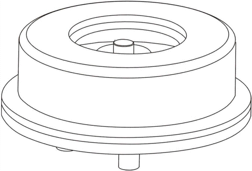
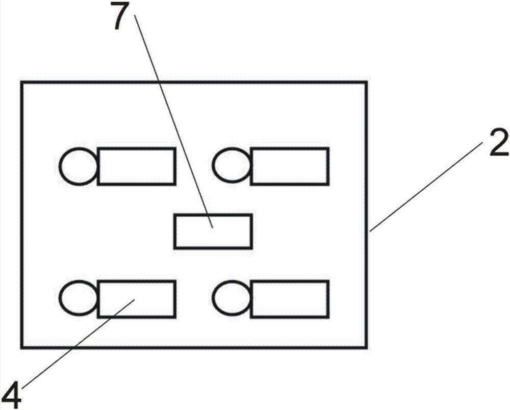
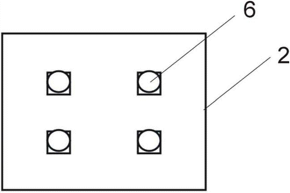
[0028] A kind of VCSEL manufacturing process of SMD miniaturization package, manufacturing process comprises:

[0029] (1) Aluminum nitride base plate: length*width*thickness: 3mm*3m...


PUM


Abstract

The invention discloses an SMD miniaturization packaged VCSEL manufacturing process. The manufacturing process comprises the steps of combining an aluminum nitride bottom plate and a kovar alloy framework together by adopting a positioning clamp; performing sintering in an oxidization atmosphere at an intermediate temperature of 700 DEG C for 70min to complete preparation of an SMD cavity; and fixing a VCSEL chip on the aluminum nitride bottom plate in a eutectic-bonding manner, enabling the VCSEL chip to be connected with a bonding pad electrode by adopting a wire binding (WB) process to complete packaging of the VCSEL chip, putting optical window glass on the SMD cavity of the packaged VCSEL chip, and sealing and fixing the optical window on the kovar alloy framework by adopting a parallel sealing and welding process to complete the manufacturing of an SMD miniaturization packaged VCSEL laser. By virtue of the manufacturing method, the volume, the length (width), height (thickness) of the laser all can be less than 5mm; and meanwhile, the laser is high in heat dissipation and can be pasted on a PCB easily, so that possibility is provided for the application of the VCSEL laser in the miniaturized products in the future.

Description

technical field [0001] The invention belongs to the packaging field of semiconductor lasers, in particular to a VCSEL manufacturing process for SMD miniaturized packaging. Background technique [0002] Lasers are more and more widely used in modern and future, and generally can be divided into solid-state lasers, gas lasers, semiconductor lasers, and fiber lasers. With the opening of the world's intelligent pattern, there is a type of laser that will show Its important position is that semiconductor lasers, due to their superior performance, low cost, small size, and rich wavelengths, will play an important role in future intelligent products, such as optical communications, big data transmission, smart phones, smart phones Home, unmanned driving (lidar) and other fields will be widely used. [0003] Due to the sensitivity of semiconductor laser chips to environmental moisture, harmful gases and pollutants, such devices often require hermetic packaging. The PN junction temp...

Claims


Application Information

Patent Timeline
Patent Type & Authority Applications(China)
IPC IPC(8): H01S5/024H01S5/022
CPCH01S5/02476H01S5/023H01S5/0233H01S5/0235H01S5/02355
Inventor 温惟善
Owner GUANGDONG GASTIGHT HERMETICAL COMPONENT
Why Eureka
Try Eureka