Split gate power MOS device

A MOS device, split gate technology, applied in semiconductor devices, electrical components, circuits, etc., can solve the problem of large overlapping area of ​​control gate and shielding gate, achieve low specific on-resistance, reduce gate-to-drain capacitance, and improve performance. Effect

Inactive Publication Date: 2017-12-26
UNIV OF ELECTRONICS SCI & TECH OF CHINA
View PDF4 Cites 4 Cited by
  • Summary
  • Abstract
  • Description
  • Claims
  • Application Information

AI Technical Summary

Problems solved by technology

The control gate and shield gate dielectric of the traditional split gate structure are made of silicon dioxide, and the overlapping area of ​​the control gate and shield gate is large, and there is still a lot of room for improvement in the gate-to-drain capacitance and the total gate charge.

Method used


Image

  • Split gate power MOS device
  • Split gate power MOS device

Examples


Embodiment 1

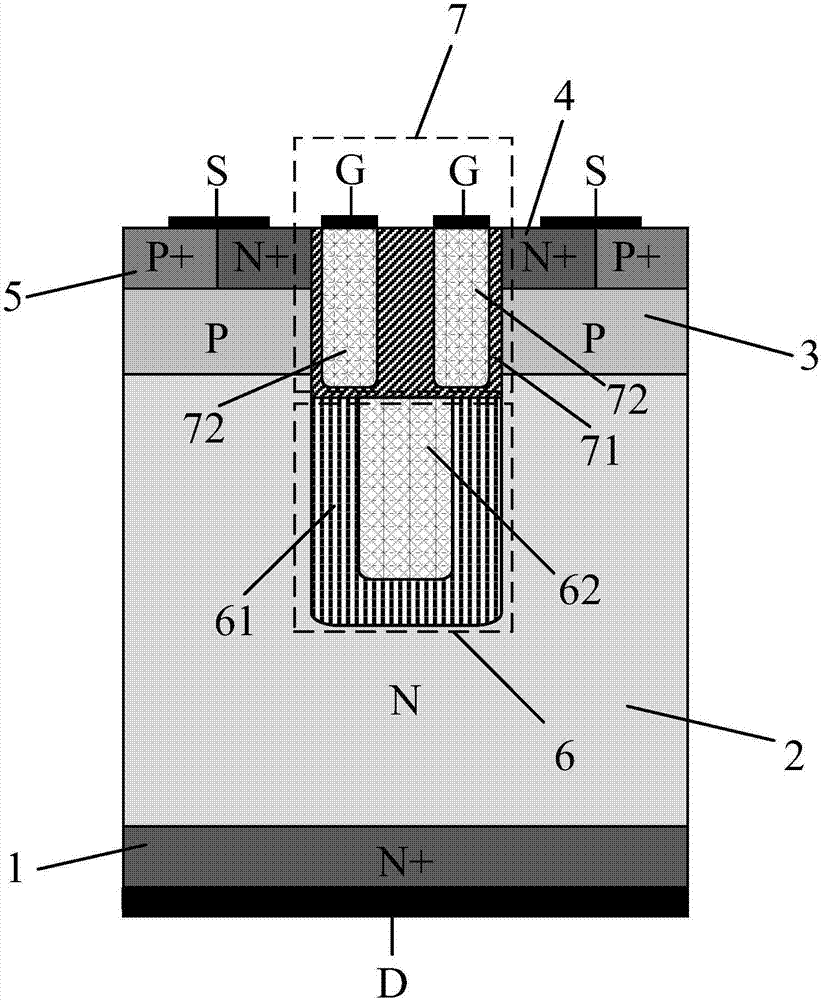
[0012] Such as figure 1 As shown, it is a structural schematic diagram of this example. Compared with the traditional split gate structure, the present invention introduces a high-K dielectric as the gate dielectric layer of the shielding gate, and divides the control gate above the shielding gate into two parts. When it is off, the high-K medium enhances the auxiliary depletion of the drift region, which increases the concentration of the drift region, which is beneficial to reduce the specific on-resistance; when it is forward-conducting, an electron accumulation layer is generated in the drift region close to the high-K medium, and the high-K medium enhances the accumulation. effect, further reducing the specific on-resistance. During the switching process of the device, the control gate and the shield gate are strongly coupled through a high-K dielectric, which greatly reduces the gate-drain capacitance; at the same time, the discrete control gate reduces the overlapping a...

Embodiment 2

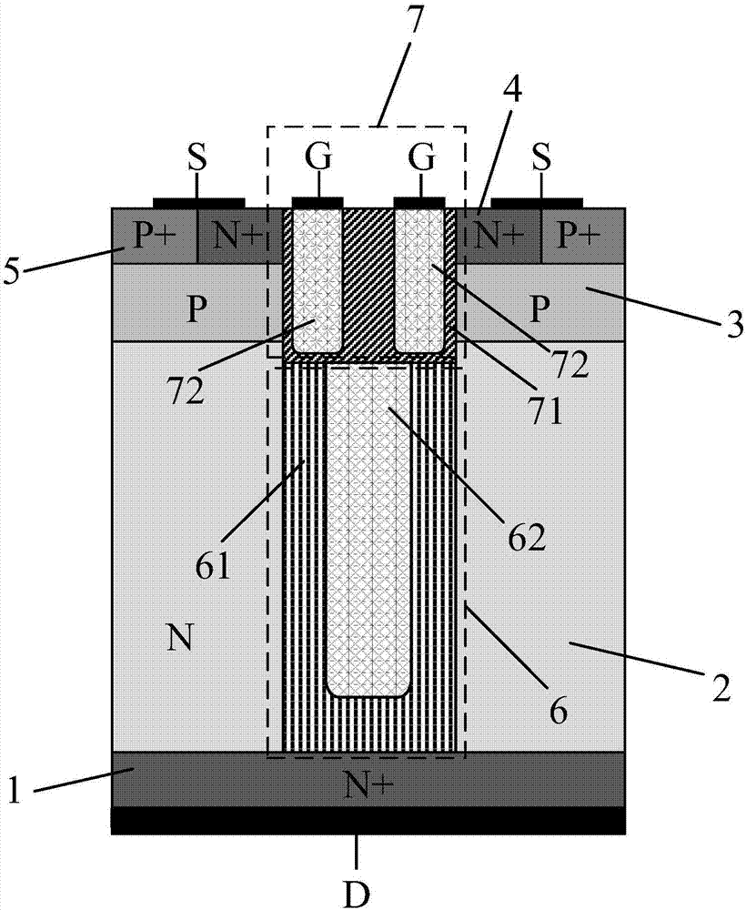
[0014] Such as figure 2 As shown, the difference between this example and Example 1 is that the lower surface of the high-K gate dielectric 61 in this example is in contact with the N-type heavily doped semiconductor substrate 1; compared with Example 1, this example can achieve a higher drift region doping The impurity concentration further reduces the specific on-resistance.


PUM


Abstract

The invention belongs to the technical field of power semiconductors and relates to a split gate power MOS device. Compared with a traditional split gate power MOS, high K medium is introduced as a gate medium layer of a shielding gate and a control gate above the shielding gate is divided into two. When the device is in forward direction blocking, the enhancement of the high K medium assists depletion of a drift region, the concentration of the drift region is improved and the reduction of specific on-resistance is facilitated. When the device is in forward direction conduction, the drift region adjacent to the high K medium produces an electron accumulation layer, the high K medium enhances the accumulation effect and the specific on-resistance is reduced further. When the device is in a switching process, the control gate and the shielding gate are in strong coupling through the high K medium, so that the gate drain capacitance is reduced substantially. At the same time, due to the separately arranged control gate, the overlapping area is reduced, so that the gate source capacitance and the total gate charge are reduced. Compared with the traditional split gate power MOS, the split gate power MOS device has lower specific on-resistance and gate drain charge; the QGC*RDS (on) figure of merit is improved distinctively and drive loss and switch loss are reduced.

Description

technical field [0001] The invention belongs to the technical field of power semiconductors and relates to a split gate power MOS device. Background technique [0002] Power MOSFET is a voltage control device with simple driving circuit, low driving power consumption and high operating frequency. It is widely used in the field of medium and low voltage and high frequency power electronics. [0003] The slot gate VDMOS eliminates the JFET area existing in the traditional planar gate VDMOS, increases the channel density of the device, and reduces the specific on-resistance of the device, making it widely used in power electronics such as switching power supplies and DC-DC converters. field. However, the traditional trench-gate VDMOS has a large gate-drain overlap capacitance, which affects the performance of the device and limits the application of the device under high-frequency conditions. In order to reduce the gate-to-drain capacitance and improve the performance of the ...

Claims


Application Information

Patent Timeline
Patent Type & Authority Applications(China)
IPC IPC(8): H01L29/78H01L29/423
CPCH01L29/42356H01L29/7802H01L29/7813H01L29/407
Inventor 罗小蓉赵哲言邓高强张凯孙涛杨洋张波
Owner UNIV OF ELECTRONICS SCI & TECH OF CHINA
Why Eureka
Try Eureka