Thermal field structure for growing large-sized silicon carbide monocrystal

A silicon carbide single crystal, large-scale technology, applied in the direction of single crystal growth, crystal growth, single crystal growth, etc., can solve the problems of difficult growth, delay, expensive crystal, etc., to avoid crystal melting, reduce cracking, and improve quality. Effect

Pending Publication Date: 2018-01-19
HARBIN AURORA OPTOELECTRONICS TECH
View PDF7 Cites 12 Cited by
  • Summary
  • Abstract
  • Description
  • Claims
  • Application Information

AI Technical Summary

Problems solved by technology

At present, the size of silicon carbide single crystal growth is small, and the growth is more difficult, which leads to more expensive crystals and delays the development of silicon carbide crystal materials. Therefore, the growth of large-size, high-quality silicon carbide single The development of crystal materials is of great significance

Method used


Image

  • Thermal field structure for growing large-sized silicon carbide monocrystal
  • Thermal field structure for growing large-sized silicon carbide monocrystal
  • Thermal field structure for growing large-sized silicon carbide monocrystal

Examples


Embodiment Construction

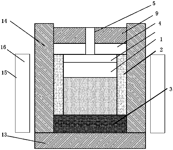
[0021] The present invention is described in detail below in conjunction with accompanying drawing:

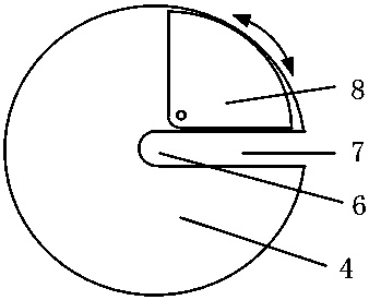
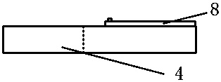
[0022] combine figure 1 The structure of this embodiment consists of a crucible 1, a crucible cover 4, a seed rod 5, an upper insulation layer structure 9, a lower insulation layer structure 13, a side insulation layer structure 14 and an induction coil structure 15. The crucible 1 is divided into two parts: a cylindrical bottomless structure 2 and a crucible holder 3. The cylindrical bottomless structure is placed on the upper part of the crucible holder, and the inside of the crucible is used to hold solid raw materials; the lower end of the seed crystal rod 5 is provided with a seed crystal tray 6 The structure is used to fix the seed crystal, and the seed rod can move axially through the control of the mechanical system; the crucible cover and the upper insulation structure are placed on the top of the crucible; in order to facilitate the installation of the seed rod, Fi...


PUM

PropertyMeasurementUnit
heightaaaaaaaaaa
diameteraaaaaaaaaa
thicknessaaaaaaaaaa

Abstract

The invention provides a thermal field structure for growing large-sized silicon carbide monocrystal. The structure integrally comprises a crucible, a crucible cover, a seed crystal rod, an upper insulating layer structure, a lower insulating layer structure, a lateral insulating layer structure and an induction coil, wherein the crucible is divided into a cylindrical bottomless structure and a crucible support, the cylindrical bottomless structure is put on the crucible support and is made of a high-purity graphite material, and the crucible support is made of a high-temperature-resistance insulating material; the lower end of the seed crystal rod has a seed crystal tray structure, and is moved along with height reduction of a solid raw material in the sublimating process; the induction coil structure outside the lateral insulating layer structure can be moved downwards from top, so that a reasonable interval between a growing interface of crystal and a raw material can be ensured. The thermal field structure can be used for reducing the probability of crystal fracture and effectively reducing the defects of micropipe, stress and the like inside the crystal, and realizes the growth of large-sized half-insulating silicon carbide monocrystal.

Description

technical field [0001] The invention relates to a thermal field structure for growing a large-size silicon carbide single crystal, in particular to a device structure for reverse temperature gradient control of a PVT method for growing a large-size silicon carbide crystal. Background technique [0002] As a third-generation semiconductor material, silicon carbide has the excellent characteristics of a band gap several times higher than that of traditional silicon materials, and has the characteristics of high breakdown electric field strength and good thermal stability. Electronic application fields such as aerospace, military industry, nuclear energy and other extreme environment applications have irreplaceable advantages. [0003] To sum up the advantages of silicon carbide crystals, silicon carbide will replace silicon materials in various fields in the future, so the demand for silicon carbide materials will also increase. At present, the size of silicon carbide single ...

Claims


Application Information

Patent Timeline
Patent Type & Authority Applications(China)
IPC IPC(8): C30B29/36C30B35/00
Inventor 左洪波杨鑫宏李铁袁帅
Owner HARBIN AURORA OPTOELECTRONICS TECH
Why Eureka
Try Eureka