Method for improving light emitting performance by automatically injecting Si ions to silicon-based material

A silicon-based material, ion implantation technology, applied in electrical components, semiconductor/solid-state device manufacturing, circuits, etc., can solve problems such as unpublished reports, only observable at low temperature, and low fluorescence annihilation rate.

Inactive Publication Date: 2018-01-19
YUNNAN UNIV
View PDF4 Cites 0 Cited by
  • Summary
  • Abstract
  • Description
  • Claims
  • Application Information

AI Technical Summary

Problems solved by technology

At present, some samples with better luminescence performance have been obtained through ion implantation. Although these research progresses play a decisive role in improving the luminescence of silicon-based materials, their external quantum efficiency is still only about one thousandth of that of GaAs devices, and Most of the luminescence can only be observed at low temperature, which is still some distance away from the practical application of Si-based optoelectronic integration.
Therefore, finding a silicon-based material with concentrated wavelength band, high luminous efficiency, low fluorescence annihilation rate and good temperature stability through self-ion implantation has become an urgent problem to be solved.
[0004] Through document retrieval, do not see the public report identical with the present invention

Method used


Image

  • Method for improving light emitting performance by automatically injecting Si ions to silicon-based material
  • Method for improving light emitting performance by automatically injecting Si ions to silicon-based material
  • Method for improving light emitting performance by automatically injecting Si ions to silicon-based material

Examples


Embodiment 1

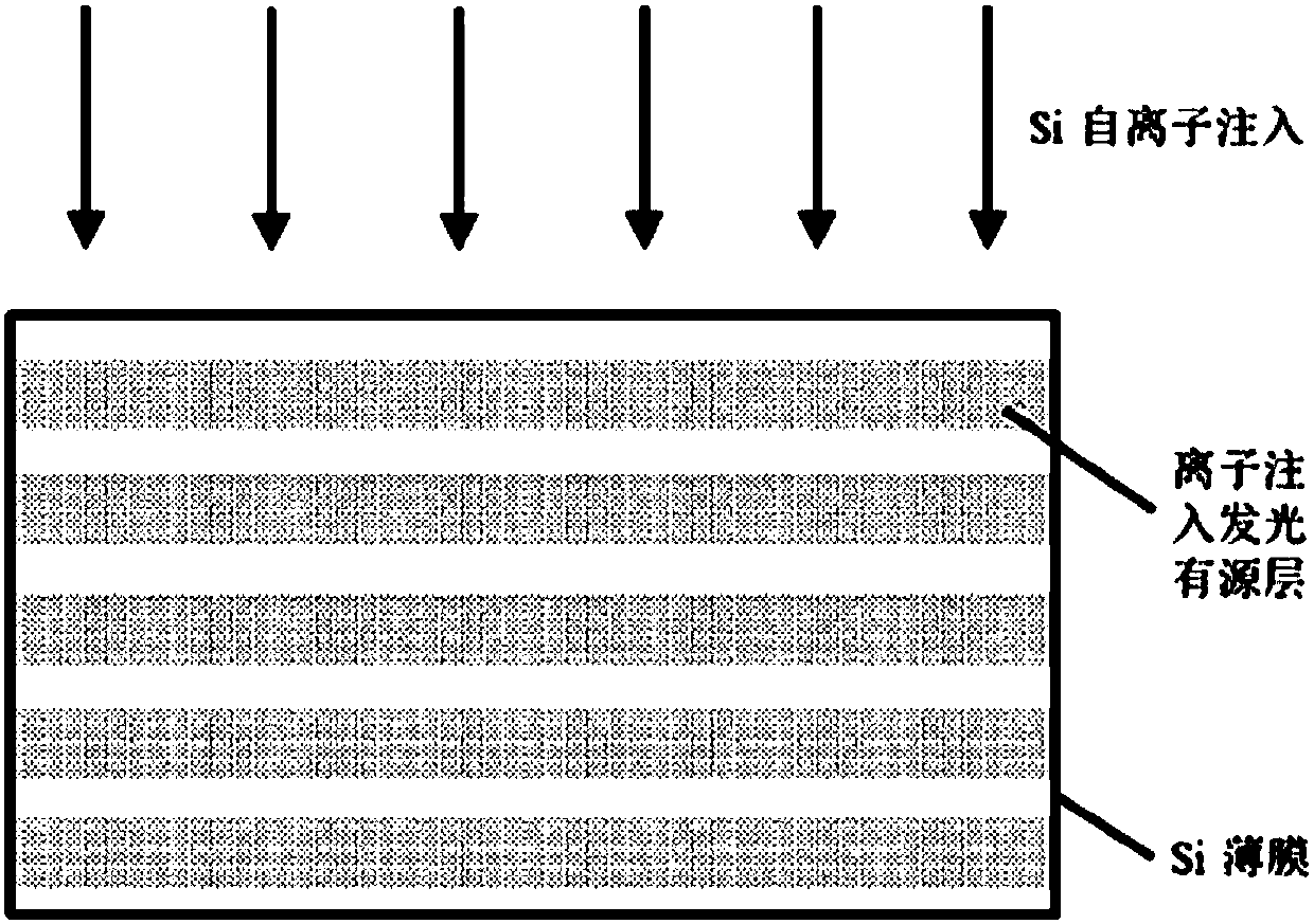
[0017] In this embodiment, Si+ is self-injected into the silicon film on the insulating layer, that is, the SOI (Silicon on insulator) substrate. The thickness of the top silicon layer is 210nm, the purity is ~99.999%, the resistivity is ~10Ω·cm, [100] crystal orientation, p type single crystal. The middle layer is 340nm thick SiO2, and the bottom layer is p-type single crystal Si with a thickness of 675 µm.

[0018] Step 1: Surface-treat the SOI substrate with Shiraki standard cleaning.

[0019] Step 2: Send the SOI substrate into the vacuum implantation chamber of the ion implanter equipment. Use an ion implanter to self-implant Si+ into the top silicon film of SOI three times. The first implantation energy is 110keV, the second implantation energy is 80keV, the third implantation energy is 50keV, and each implantation dose is 1×1014cm-2 . The included angle between the ion beam and the surface normal of the silicon thin film layer is 7°, and the whole implantation proces...

Embodiment 2

[0023] Step 1 is the same as in Example 1.

[0024] The difference between step 2 and embodiment 1 is that Si+ is self-implanted into SOI top layer silicon three times with an ion implanter, and the implantation dose is 1×1013 cm-2 each time.

[0025] The difference between step 3 and embodiment 1 is that a rapid thermal annealing furnace is used to anneal the SOI substrate after ion implantation, the annealing time is 60s, and the annealing temperature is 300°C.

Embodiment 3

[0027] In this embodiment, a p-type [100] oriented single-crystal Si substrate is used, with a thickness of 675 μm, a purity of ~99.999%, and a resistivity of ~10Ω·cm.

[0028] Step 1: Surface-treat the p-type Si substrate with Shiraki standard cleaning.

[0029] Step 2: Send the Si substrate into the vacuum implantation chamber of the ion implanter equipment. Use an ion implanter to self-implant Si+ into the silicon thin film layer five times. The first implantation energy is 250keV, the second implantation energy is 200keV, the third implantation energy is 140keV, the fourth implantation energy is 100keV, and the fifth implantation energy is 100keV. The implantation energy is 60keV, and the implantation dose is 1×1016cm-2 each time. The included angle between the ion beam and the surface normal of the silicon thin film layer is 7°, and the whole implantation process is carried out under vacuum and room temperature.

[0030] Step 3: Perform conventional annealing on the imp...


PUM

PropertyMeasurementUnit
Thicknessaaaaaaaaaa
Resistivityaaaaaaaaaa
Thicknessaaaaaaaaaa

Abstract

The invention provides a method for improving light emitting performance by automatically injecting Si ions to a silicon-based material. Based on an ion injection and annealing technology, 3-5 times of Si automatic ion injection of different energy is performed on a silicon thin film of the silicon-based material which refers to an Si substrate or an SOI substrate with the cleaned surface; and next, different parameters of the conventional annealing or quick thermal annealing can be adjusted to obtain the silicon-based light emitting material with excellent light emitting performance. The method has the core that the ion injection technology is adopted, and Si automatic ion injection is performed at the same dosage in an energy gradual decreasing mode, so that ion injection active layer thickness is improved, and the silicon-based light emitting material with high light emitting efficiency, low fluorescence annihilating speed and high temperature stability is achieved.

Description

technical field [0001] The invention relates to a method for improving luminous performance by implanting Si ions into silicon-based materials, and belongs to the field of preparation of silicon-based luminescent materials. Background technique [0002] Due to its indirect bandgap properties, the radiative recombination luminescence of silicon-based materials usually needs to be assisted by phonons, which has caused it to stagnate in the field of optoelectronic integration. At present, in order to improve the luminescent properties of silicon-based materials, the way of modifying their luminescence by defect engineering has become a major focus of research in the field of materials science. Defect engineering is represented by ion implantation. Defects are introduced into crystal Si through ion implantation. Different types of defects and clusters can form impurity (or defect) sub-levels with different positions and widths in the forbidden band, so that the electrons in the ...

Claims


Application Information

Patent Timeline
IPC IPC(8): H01L21/265H01L21/322H01L21/324
Inventor 王茺欧阳凌曦周蒙薇王荣飞杨杰邱锋杨宇
Owner YUNNAN UNIV
Why Eureka
Try Eureka