Mixed annealing apparatus and annealing method
An annealing device and annealing technology, applied in the manufacturing of electrical components, circuits, semiconductor/solid-state devices, etc., can solve the problems of reducing the steepness of the diffusion region, uncontrollable edges of the diffusion region, and product damage, etc., to improve the efficiency of microwave annealing, Good absorption, avoid damage effect
- Summary
- Abstract
- Description
- Claims
- Application Information
AI Technical Summary
Problems solved by technology
Method used
Image


Examples
specific example
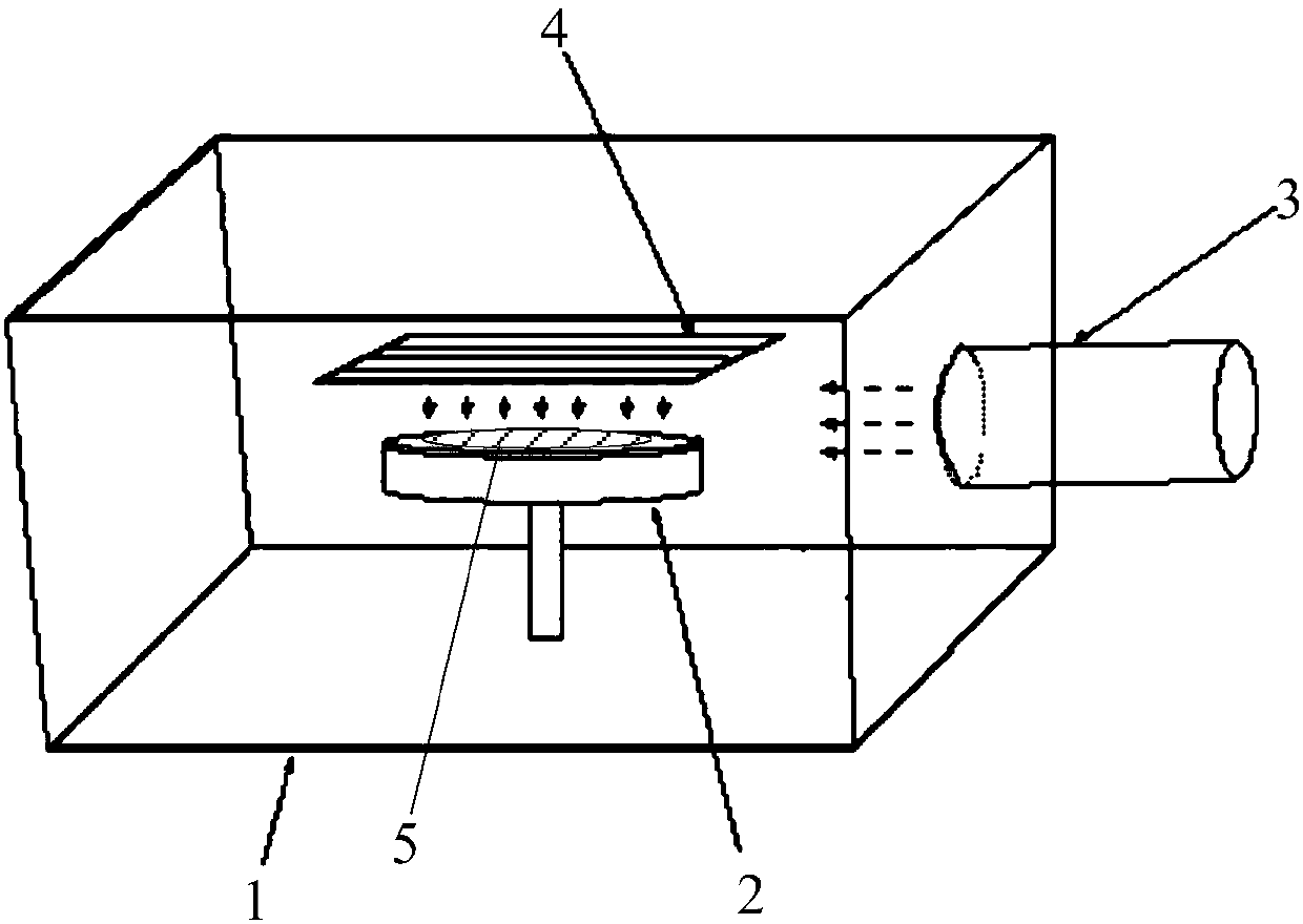
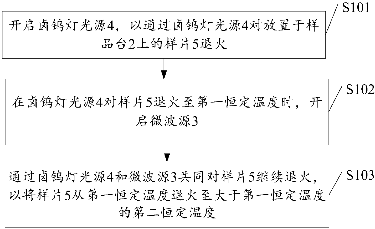
[0052] Set the power of the tungsten-halogen light source 4 to 2KW, and the irradiation time is 7 minutes, so that the tungsten-halogen light source 4 anneals the sample 5 in the sample chamber 1 at 2KW for 5 minutes, so that the sample 5 reaches the first constant temperature . Turn on the microwave source 3, set the microwave power of the microwave source 3 to 3KW and the application time to 2 minutes, the microwave source 3 and the tungsten halogen lamp light source 4 jointly anneal the sample 5 for 2 minutes, so that the sample 5 reaches the second constant temperature .
[0053] In this example, the annealing duration of the entire annealing process is 7 minutes. The first 5 minutes are heated by the tungsten halogen light source 4 alone, and the second 2 minutes are jointly heated by the tungsten halogen light source 4 and the microwave source 3 . Due to the irradiation of the tungsten-halogen lamp in the first 5 minutes, the dielectric constant of the local area of ...
PUM
 Abstract
Description
Claims
Application Information
 - R&D Engineer
- R&D Manager
- IP Professional
- Industry Leading Data Capabilities
- Powerful AI technology
- Patent DNA Extraction
Browse by: Latest US Patents, China's latest patents, Technical Efficacy Thesaurus, Application Domain, Technology Topic.
© 2024 PatSnap. All rights reserved.Legal|Privacy policy|Modern Slavery Act Transparency Statement|Sitemap