Supercharge Your Innovation With Domain-Expert AI Agents!

Silicon through hole interconnection structure, preparation method of silicon through hole interconnection structure and silicon through hole radio-frequency transmission structure

A technology of interconnection structure and radio frequency transmission, which is applied in semiconductor/solid-state device manufacturing, electrical components, electric solid-state devices, etc. It can solve problems such as poor high-frequency transmission performance and large TSV stress, achieve excellent transmission performance, and increase channel-to-channel Isolation, the effect of realizing three-dimensional integration

Pending Publication Date: 2018-02-16
CHENGDU GANIDE TECH
View PDF0 Cites 6 Cited by
  • Summary
  • Abstract
  • Description
  • Claims
  • Application Information

AI Technical Summary

Problems solved by technology

[0005] In order to solve the problems existing in the prior art, the first object of the present invention is to provide a through-silicon via interconnection structure, which realizes the electrical interconnection path vertically penetrating through the microelectronic chip body, and supports chip-level three-dimensional stacked integration and packaging. Solve the shortcomings of the traditional all-copper filled TSV with high stress and poor high-frequency transmission performance, and realize a high-reliability, low-loss RF vertical interconnection structure

Method used


Image

  • Silicon through hole interconnection structure, preparation method of silicon through hole interconnection structure and silicon through hole radio-frequency transmission structure
  • Silicon through hole interconnection structure, preparation method of silicon through hole interconnection structure and silicon through hole radio-frequency transmission structure
  • Silicon through hole interconnection structure, preparation method of silicon through hole interconnection structure and silicon through hole radio-frequency transmission structure

Examples


Embodiment

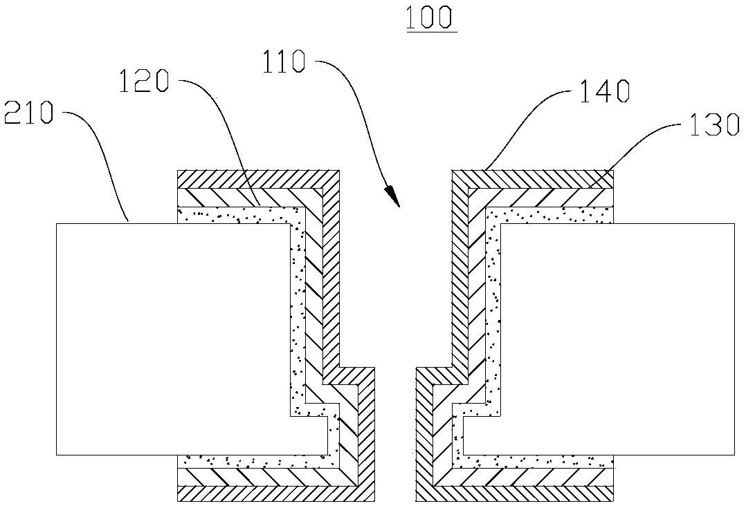
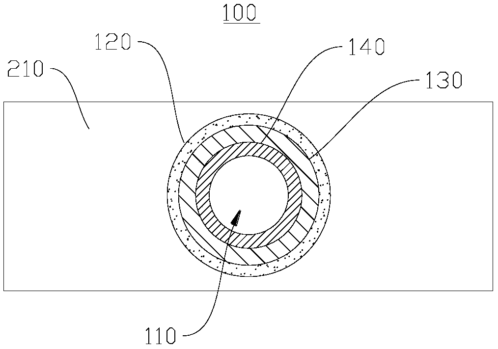
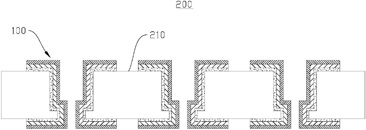
[0050] See figure 1 and figure 2 The shown TSV interconnection structure 100 of the present invention includes a TSV 110 penetrating a silicon substrate 210, an insulating layer 120 disposed on the sidewall of the TSV 110, and a metal layer disposed on the surface of the insulating layer 120. The copper layer 130 and the passivation layer 140 disposed on the surface of the metal copper layer 130 . Such as figure 1 and 2 As shown, the insulating layer 120 , the metal copper layer 130 and the passivation layer 140 form a coaxial structure with the center line of the TSV 110 as the axis. In this embodiment, the insulating layer 120 is made of silicon dioxide; the passivation layer 140 is made of gold. The thickness of the metallic copper layer 130 in this embodiment is 6-15 μm, preferably 8-12 μm, more preferably 10 μm. In this embodiment, the TSVs 110 are vertical holes or tapered holes. It should be noted that the tapered hole referred to in the present invention include...


PUM

PropertyMeasurementUnit
Thicknessaaaaaaaaaa

Abstract

The invention discloses a silicon through hole interconnection structure, a preparation method of the silicon through hole interconnection structure and a silicon through hole radio-frequency transmission structure, and belongs to the field of integrated packaging and signal transmission. The silicon through hole interconnection structure comprises a silicon through hole configured to penetrate through a silicon substrate, an insulating layer arranged on the side wall of the silicon through hole, a metal copper layer arranged on the surface of the insulating layer and a passivation layer arranged on the surface of the metal copper layer. The insulating layer, the metal copper layer and the passivation layer form a coaxial structure with the central line of the silicon through hole as the axis thereof. The silicon through hole radio-frequency transmission structure comprises a silicon substrate and a plurality of the above silicon through hole interconnection structures. The plurality of silicon through hole interconnection structures are arranged on the silicon substrate. According to the invention, the chip-level three-dimensional stacked integrating and packaging is realized, while the defects in the prior art that the traditional full-copper-filling type TSV is large in stress and poor in high-frequency transmission performance are overcome at the same time. A radio-frequency vertical interconnection structure, high in reliability and low in loss, is realized.

Description

technical field [0001] The invention relates to the fields of integrated packaging and signal transmission, in particular to a through-silicon hole interconnection structure, a preparation method thereof, and a through-silicon hole radio frequency transmission structure. Background technique [0002] In the complex battlefield electromagnetic environment, how to better play the role of electronic information equipment and achieve good combat effectiveness has become more difficult, and put forward higher requirements for the intelligence, miniaturization, and lightweight of electronic information equipment. [0003] TSV (through silicon via) technology is the abbreviation of through-silicon via technology, generally referred to as through-silicon via technology, and is a technical solution for interconnection of stacked chips in three-dimensional integrated circuits. TSV technology has the advantages of small size, high density, high integration, and small interconnection de...

Claims


Application Information

Patent Timeline
IPC IPC(8): H01L23/538H01L23/552H01L23/66H01L21/768
CPCH01L23/5384H01L23/552H01L23/66H01L21/76898
Inventor 何舒玮童伟陈依军胡柳林吕继平王栋唐仲俊
Owner CHENGDU GANIDE TECH
Features
  • R&D
  • Intellectual Property
  • Life Sciences
  • Materials
  • Tech Scout
  • Unparalleled Data Quality
  • Higher Quality Content
  • 60% Fewer Hallucinations
Learn More