Novel resistive random access memory and manufacturing method therefor

A resistive memory and resistive switching technology, applied in electrical components and other directions, can solve the problems of improving the performance regulation of resistive memory, affecting the stability of resistive memory cells, and complicating the resistance switching mechanism, and achieving excellent resistance transition characteristics. , the effect of abundant reserves and stable resistance transformation characteristics

Active Publication Date: 2018-02-23
ZHEJIANG NORMAL UNIVERSITY
View PDF6 Cites 0 Cited by
  • Summary
  • Abstract
  • Description
  • Claims
  • Application Information

AI Technical Summary

Problems solved by technology

[0005] However, there are still several problems in the preparation of transition metal oxide resistive memory by using standard CMOS integrated circuit technology: the raw materials of the resistive dielectric layer currently used are rare elements, with limited reserves and high prices; The influence of the mechanism complicates the resistive switching mechanism and increases the difficulty of controlling the performance of the resistive variable memory; if the resistive variable memory unit, especially the resistive variable dielectric layer, is in contact with air, the oxygen or water vapor in the air will adhere to the resistive variable memory. around the dielectric layer, and then diffuse into the resistive dielectric layer to affect the stability of the resistive memory unit

Method used


Image

  • Novel resistive random access memory and manufacturing method therefor
  • Novel resistive random access memory and manufacturing method therefor
  • Novel resistive random access memory and manufacturing method therefor

Examples


Embodiment Construction

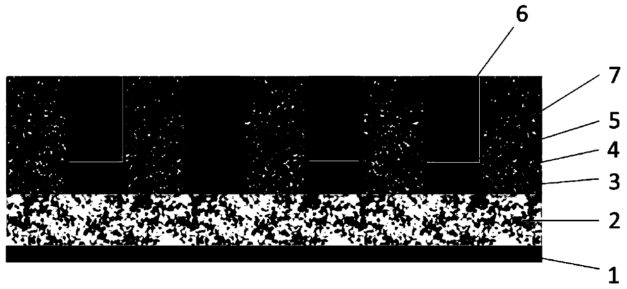
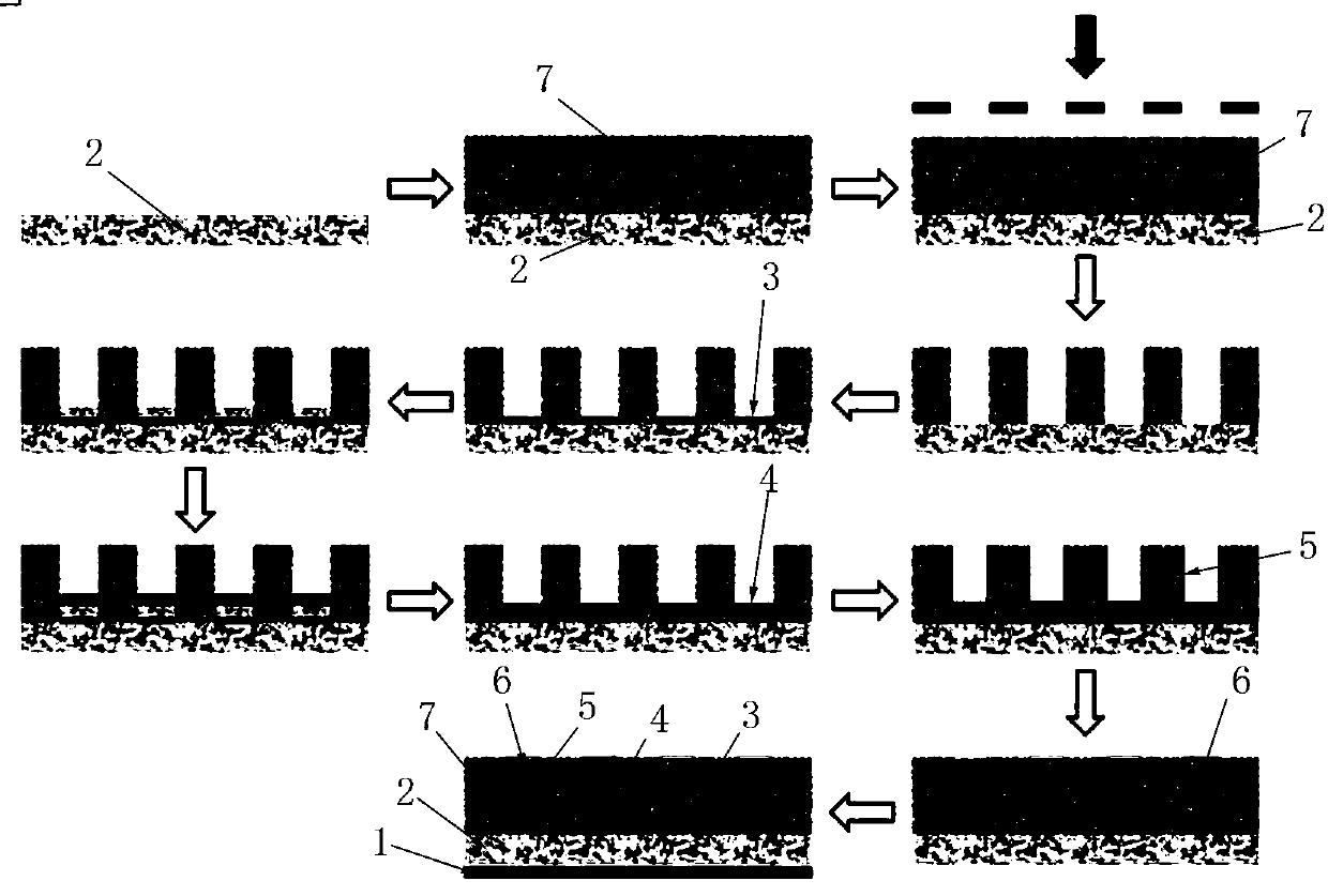
[0027] See attached picture. The resistive variable memory described in this embodiment includes a silicon wafer substrate 2 and a back electrode 1, a silicon dioxide protective layer 7 is provided above the silicon wafer substrate 2, and several cylindrical recesses are etched on the silicon dioxide protective layer 7, The contact between the recess and the silicon wafer substrate is a resistive dielectric layer 3, and above the resistive dielectric layer 3 is a silicide layer 4, and above the silicide layer 4 and the inner wall of the corresponding recess is an anti-metal diffusion layer 5. Inside the metal diffusion layer 5 is a metal top electrode 6; the resistive dielectric layer 3 is a silicon-based thin film, and the anti-metal diffusion layer 5 is a tantalum / tantalum nitride mixed layer.

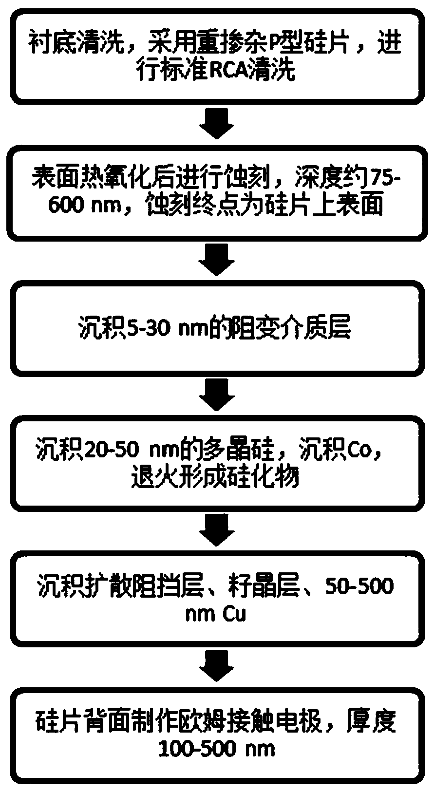
[0028] The preparation process of the resistive variable memory described in this embodiment:

[0029] 1) First, use the RCA standard cleaning method in the integrated circuit (IC) ...


PUM


Abstract

The invention discloses a novel resistive random access memory and a manufacturing method therefor. The novel resistive random access memory comprises a silicon wafer substrate and a back electrode; asilicon dioxide protection layer is arranged on the silicon wafer substrate; a plurality of cylindrical concave holes are etched in the silicon dioxide protection layer; a resistive random dielectriclayer is positioned in the contact place between the concave holes and the silicon wafer substrate; a silicide layer is arranged on the resistive random dielectric layer; a metal diffusion preventionlayer is arranged on the silicide layer and on the circumferential inner wall corresponding to the concave holes; and a metal top electrode is arranged in the metal diffusion prevention layer. The resistive random access memory unit obtained in the invention has excellent and stable resistance conversion characteristic; and by virtue of introduction of the silicide layer, the potential barrier resistance between an upper electrode and the resistive random dielectric layer is lowered, and the resistive random dielectric layer is subjected to resistance conversion without being influenced by the upper electrode material, so that the stability of the memory unit is further improved.

Description

technical field [0001] The invention belongs to the technical field of ultra-large-scale integrated circuits, and in particular relates to a novel resistive variable memory and a manufacturing method thereof. Background technique [0002] At present, the world's advanced memory manufacturers are mass-producing 3D NAND memory. This is because the storage capacity per unit area of ​​the previous generation of planar flash memory has reached the physical limit. Due to the continuous reduction of physical size, traditional flash memory has the problem of reduced reliability due to charge leakage. In addition, people have put forward higher and higher requirements for electronic products, including key parameters such as read / erase speed, capacity, and reliability. . 3D NAND memory is developed on the basis of planar NAND memory (that is, 2D NAND memory), which has significantly improved the storage capacity of flash memory. But it is the next-generation storage technology—resi...

Claims


Application Information

Patent Timeline
Patent Type & Authority Applications(China)
IPC IPC(8): H01L45/00
CPCH10N70/801H10N70/841H10N70/011
Inventor 黄仕华陈达
Owner ZHEJIANG NORMAL UNIVERSITY
Why Eureka
Try Eureka