Semiconductor structure and manufacturing method thereof

A manufacturing method and semiconductor technology, which is applied in semiconductor/solid-state device manufacturing, semiconductor devices, electrical components, etc., can solve the problems that the electrical properties of semiconductor structures need to be improved, and achieve the effect of reducing channel leakage current and improving electrical performance

Inactive Publication Date: 2018-03-09
SEMICON MFG INT (SHANGHAI) CORP +1
View PDF5 Cites 15 Cited by
  • Summary
  • Abstract
  • Description
  • Claims
  • Application Information

AI Technical Summary

Problems solved by technology

[0006] However, even if the FinFET structure is introduced in the ultra-shallow junction technology, the electrical performance of the prior art semiconductor structure still needs to be improved.

Method used


Image

  • Semiconductor structure and manufacturing method thereof
  • Semiconductor structure and manufacturing method thereof
  • Semiconductor structure and manufacturing method thereof

Examples


Embodiment Construction

[0035] It is known from the background technology that the electrical performance of the semiconductor structure needs to be improved. The reasons are:

[0036] In order to improve the short-channel effects (SCE: short-channel effects) and reduce the increase of the channel leakage current of the transistor, generally the method of reducing the injection energy of the light doping (LDD) process is adopted; or, the pre-amorphization doping is adopted Pre-amorphization Implantation (PAI) process to achieve the purpose of ultra shallow junction (Ultra Shallow Junction, USJ), thereby reducing the channel leakage current of the semiconductor structure and reducing the short channel effect.

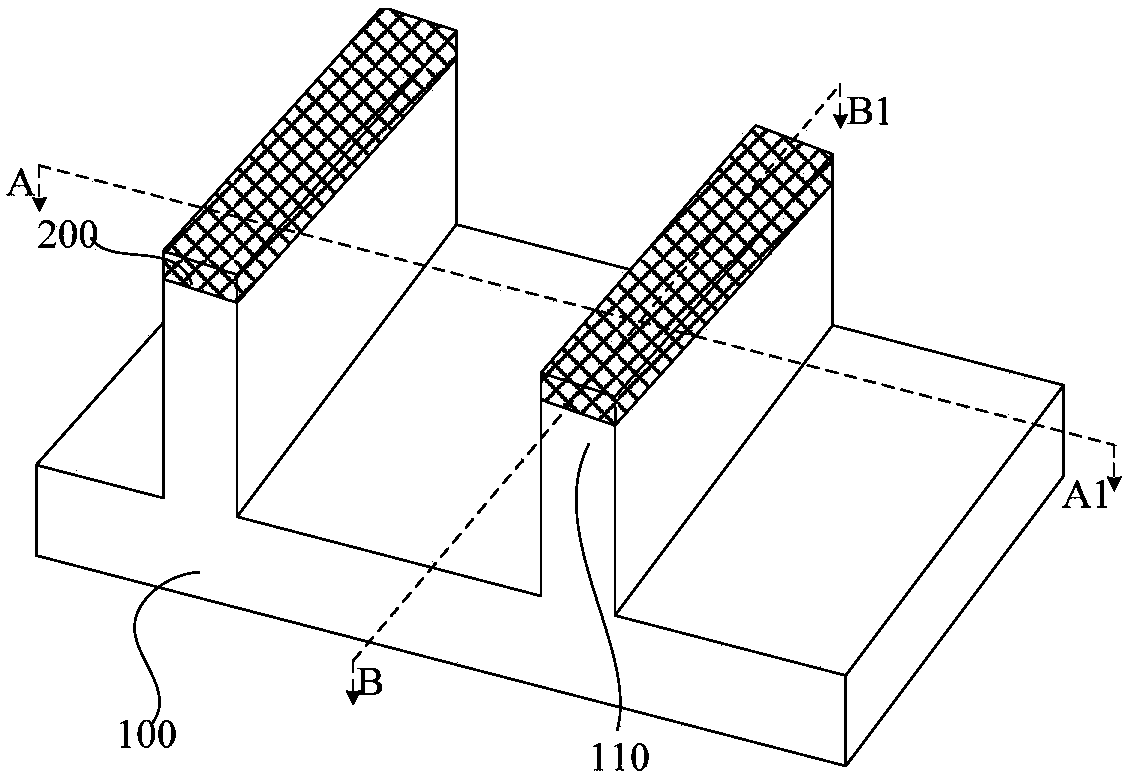
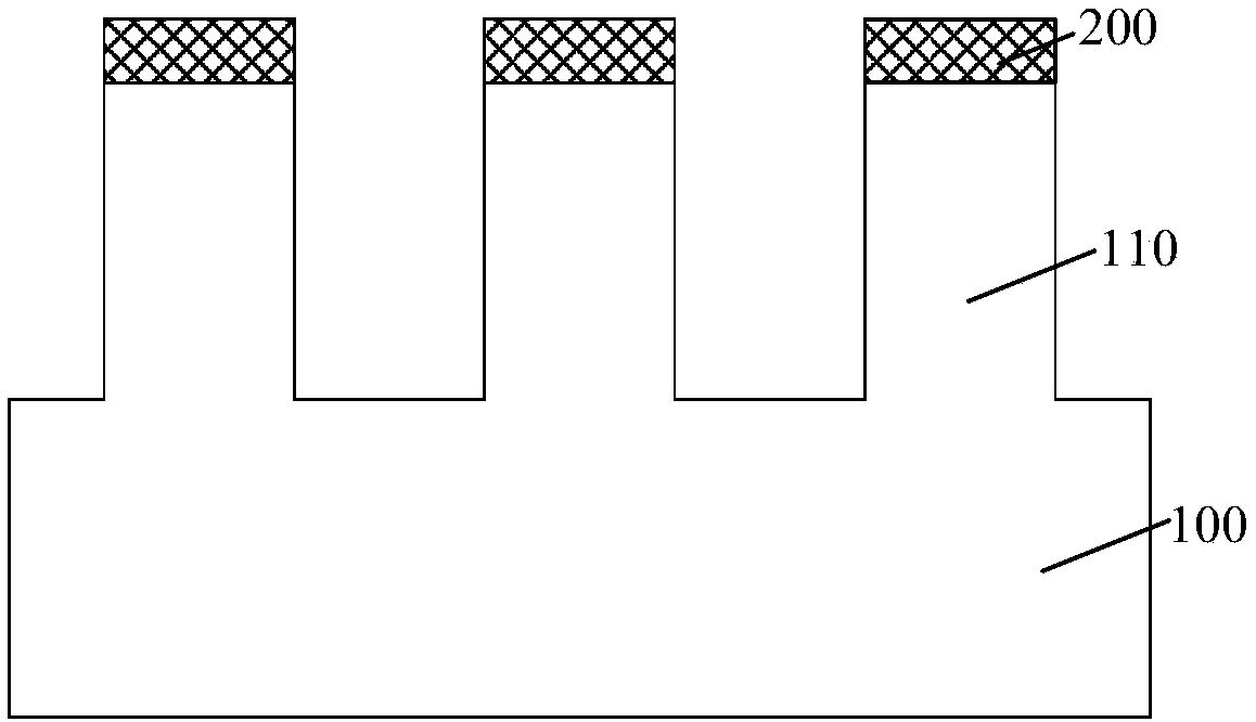
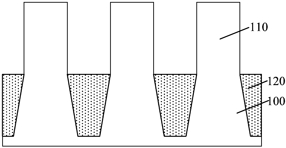
[0037] However, after the introduction of the FinFET structure, due to the three-dimensional structure limitation, it is difficult to do the doping process on the bottom of the fin portion, so that the bottom punch through of the source and drain doped regions is likely to occur, and it is difficult...


PUM


Abstract

The invention discloses a semiconductor structure and a manufacturing method thereof. The method comprises steps: a base is provided, wherein the base comprises a substrate and fin parts protruding against the substrate; a gate structure which crosses over the fin parts and covers the top surfaces and the side wall surfaces of part of the fin parts is formed; the fin parts at two sides of the gatestructure are removed, and grooves with the substrate exposed are formed at two sides of the gate structure; the substrate at the bottom part of the groove is internally provided with an anti-diffusion doping area; and after the anti-diffusion doping area is formed, a stress layer is formed in the groove, and a source-drain doping area is formed in the stress layer. After the grooves with the substrate exposed are formed at two sides of the gate structure, the substrate at the bottom part of the groove is internally provided with the anti-diffusion doping area; later, after the stress layer is formed in the groove and the source-drain doping area is formed in the stress layer, the anti-diffusion doping area is located in the substrate at the bottom part of the source-drain doping area, the anti-diffusion doping area can suppress diffusion of doping ions of the source-drain doping area to a channel area, bottom through can be prevented from happening to the source-drain doping area, and channel leakage current can thus be reduced.

Description

Technical field [0001] The present invention relates to the field of semiconductors, in particular to a semiconductor structure and a manufacturing method thereof. Background technique [0002] With the continuous development of semiconductor process technology, the development trend of semiconductor process nodes following Moore's Law continues to decrease. In order to adapt to the reduction of process nodes, the channel length of the MOSFET has to be continuously shortened. The shortening of the channel length has the advantages of increasing the die density of the chip and increasing the switching speed of the MOSFET. [0003] However, as the channel length of the device is shortened, the distance between the source and the drain of the device is also shortened. As a result, the ability of the gate to control the channel becomes worse, causing subthreshold leakage, namely The so-called short-channel effects (SCE: short-channel effects) are more likely to occur, which increases...

Claims


Application Information

Patent Timeline
Patent Type & Authority Applications(China)
IPC IPC(8): H01L21/336H01L29/78H01L29/10
Inventor 赵猛
Owner SEMICON MFG INT (SHANGHAI) CORP
Why Eureka
Try Eureka