SOI-RC-LIGBT device and preparation method thereof

A device, N-type technology, applied in the field of power semiconductor devices, can solve the problem that IGBT cannot be fully turned on, and achieve the effects of eliminating the Snapback phenomenon, improving the distribution of the electric field, and increasing the breakdown voltage

Active Publication Date: 2018-03-09
UNIV OF ELECTRONICS SCI & TECH OF CHINA
View PDF7 Cites 17 Cited by
  • Summary
  • Abstract
  • Description
  • Claims
  • Application Information

AI Technical Summary

Problems solved by technology

This will prevent the IGBTs from being fully turned on i

Method used


Image

  • SOI-RC-LIGBT device and preparation method thereof
  • SOI-RC-LIGBT device and preparation method thereof
  • SOI-RC-LIGBT device and preparation method thereof

Examples


Embodiment 1

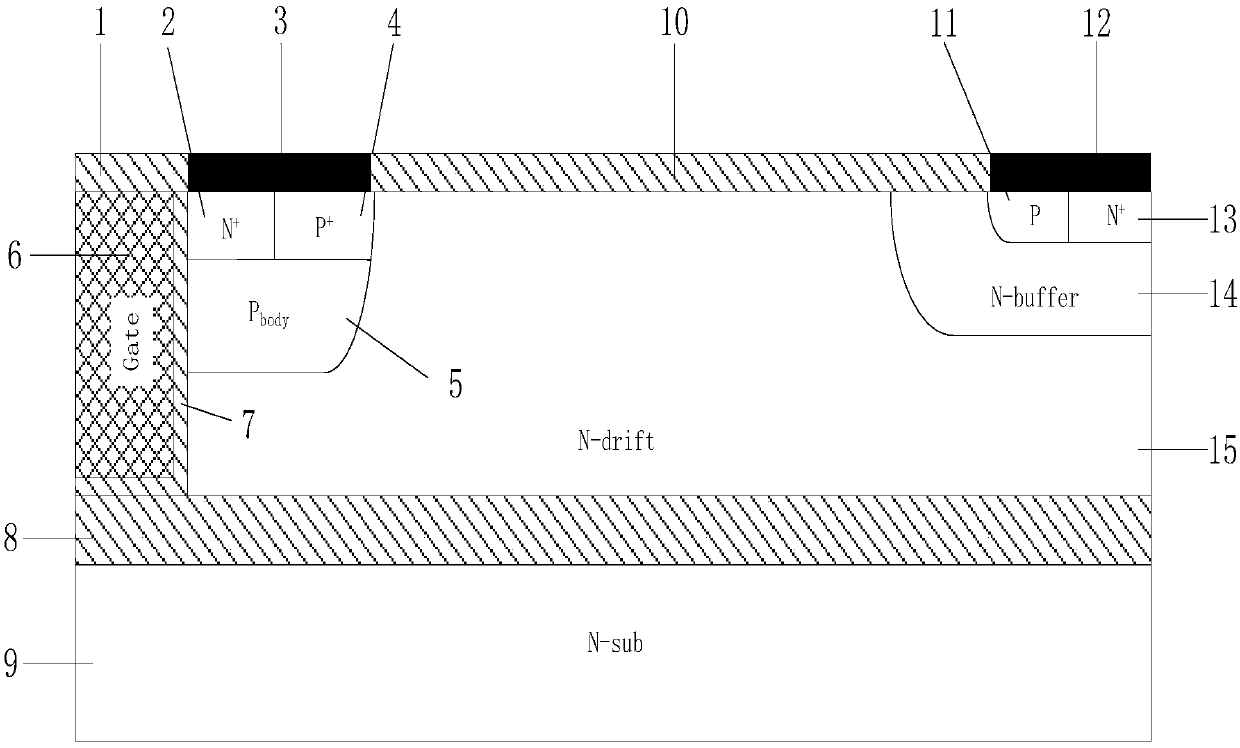
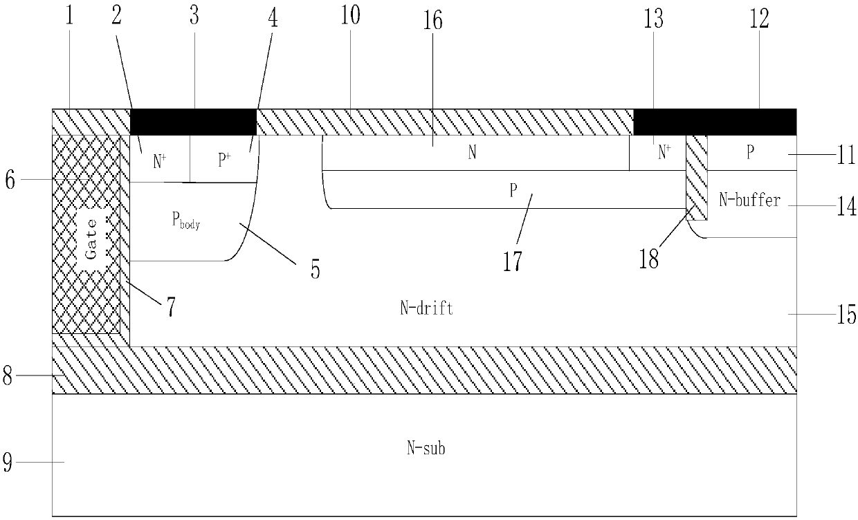
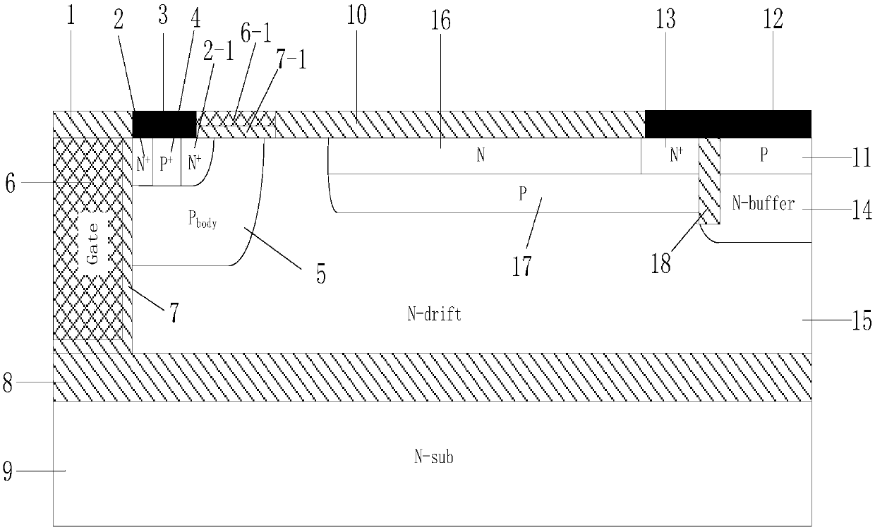
[0048] An SOI-RC-LIGBT device, comprising: an N-type substrate 9, a buried oxide layer 8, and an N-type drift region 15 arranged sequentially from bottom to top; one end of the N-type drift region 15 is provided with a gate dielectric layer 7 A trench gate structure composed of a gate electrode 6, the gate electrode 6 is located inside one side of the gate dielectric layer 7; the other side of the gate dielectric layer 7 inside the N-type drift region 15 is provided with a P-type base region 5, N is provided above the inside of the P-type base region 5 + source region 2 and P + contact region 4, the P-type base region 5 and the N + The sides of the source region 2 are in contact with the sides of the gate dielectric layer 7; the N + source region 2 and P +There is an emitter 3 above the contact region 4, an oxide layer 1 above the gate dielectric layer 7 and the gate electrode 6; an N-type buffer zone 14 is provided at the end of the N-type drift region 15 away from the tre...

Embodiment 2

[0052] This embodiment is basically the same as Embodiment 1, except that the P-type buried layer 17 is composed of a plurality of regions whose concentrations decrease from left to right.

Embodiment 3

[0054] This embodiment is basically the same as Embodiment 1, except that the N-type strip 16 is composed of a plurality of regions whose concentrations increase from left to right.


PUM

PropertyMeasurementUnit
Thicknessaaaaaaaaaa
Depthaaaaaaaaaa
Thicknessaaaaaaaaaa

Abstract

The invention provides an SOI-RC-LIGBT device and a preparation method thereof. The SOI-RC-LIGBT device comprises an N-type substrate, a buried oxide layer, an N-type drift region, a trench gate structure, a P-type base region, an N+ source region, a P+ contact region, an emitting electrode, an oxide layer, an N-type buffer region and a P-type collector region; an N-type strip is arranged on the surface of the portion, between the P-type base region and the N-type buffer region, of the N-type drift region, and a P-type buried layer is arranged in the portion, below the N-type strip, of the drift region; a medium trench structure is arranged between the right sides of the N-type strip and the P-type buried layer and the left sides of the N-type buffer region and the P-type collector region;an N+ collector region is arranged between the N-type strip and the medium trench structure. According to the SOI-RC-LIGBT device, while the IGBT conduction characteristic snapback phenomena are eliminated, the breakdown voltage of the device is improved, the forward conduction voltage drop of the device is reduced, the shutoff speed is increased, the shutoff loss is reduced, and meanwhile, the reverse recovery characteristics of an integrated free-wheeling diode are improved.

Description

technical field [0001] The invention belongs to the technical field of power semiconductor devices, and in particular relates to a reverse conduction lateral insulated gate bipolar transistor (RC-LIGBT) device based on SOI (Silicon On Insulator) technology and a preparation method thereof. Background technique [0002] Semiconductor power devices are the basic electronic components for energy control and conversion in power electronic systems. The continuous development of power electronics technology has opened up a wide range of application fields for semiconductor power devices. MOS-type semiconductor power devices marked by IGBT, VDMOS, and CoolMOS are the mainstream of devices in the field of power electronics today. Among them, the most representative semiconductor power device is IGBT. [0003] IGBT (Insulated Gate Bipolar Transistor, Insulated Gate Bipolar Transistor) is a voltage-controlled MOS / BJT composite device. Structurally, the structure of IGBT is very simil...

Claims


Application Information

Patent Timeline
IPC IPC(8): H01L29/739H01L29/06H01L21/331
CPCH01L29/0623H01L29/66325H01L29/7394
Inventor 张金平赵倩刘竞秀李泽宏任敏张波
Owner UNIV OF ELECTRONICS SCI & TECH OF CHINA
Why Eureka
Try Eureka