An integrated prism assembly for surface plasmon resonance detection system

A surface plasmon and resonance detection technology, applied in the field of optical detection, can solve the problems of the complex structure of traditional chips, affecting the reading of optical signals, and being unfavorable for practical promotion and use, so as to reduce costs, shorten working time, and avoid light scattering and deformation. Effect

Active Publication Date: 2020-05-15
丁利 +4
View PDF5 Cites 0 Cited by
  • Summary
  • Abstract
  • Description
  • Claims
  • Application Information

AI Technical Summary

Problems solved by technology

The incident light can only reach the metal film layer through the manually bonded "prism-coupling material interface" and "coupling material-chip interface". In the ordinary design, there are 4 more interfaces than the integrated prism, and there will be light energy loss (due to the difference in refractive index) at each interface, or it may easily cause reaction pool leakage, chip damage or coupling during operation. Bubbles, etc. are generated in the material, which affect the optical signal reading
The traditional chip structure is complex and the production process is cumbersome, which is not conducive to the actual promotion and use

Method used


Image

  • An integrated prism assembly for surface plasmon resonance detection system
  • An integrated prism assembly for surface plasmon resonance detection system
  • An integrated prism assembly for surface plasmon resonance detection system

Examples


Embodiment Construction

[0027] The structure of the integrated prism assembly of the present invention will be further described in detail below in conjunction with the accompanying drawings.

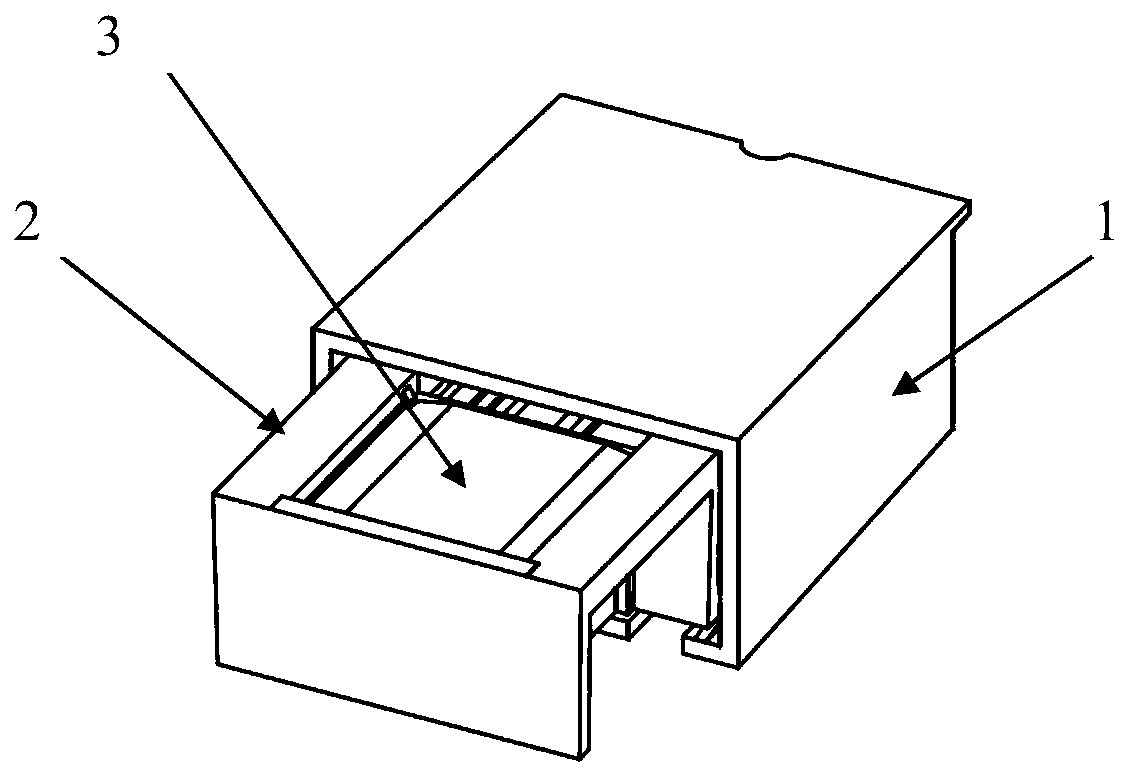
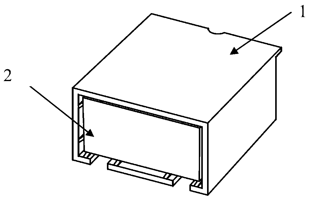
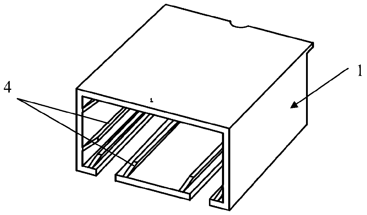
[0028] see Figure 1a-Figure 4b One embodiment of the invention is shown. The prism chip assembly in the figure includes an integrated prism chip and a corresponding chip box. The integrated prism chip can be obtained by cold processing of optical glass material, and the chip box can be formed by injection molding of plastic material. The chip box is composed of a chip card box 2 and a chip outer box 1. The chip card box 2 and the chip outer box 1 are a drawer structure. The chip card box 2 can be loaded into the chip outer box 1 and forms an independent chamber with the chip outer box 1. , to protect the chip from contamination.

[0029] The integrated prism chip 3 is columnar, and its cross section is wide at the top and narrow at the bottom. The integrated prism chip 3 has three optical surfaces, wherei...


PUM


Abstract

The invention discloses an integrated prism assembly for a surface plasmon resonance detection system. The integrated prism assembly comprises a chip outer box, a chip clamping box and an integrated prism chip. The chip outer box is a hollow regular hexahedron with front and rear open sides. The top surface of the chip clamping box is provided with an open hole. A cavity for accommodating the integrated prism chip is formed in the chip clamping box. The left and right sides of the chip clamping box are respectively provided with two through holes for allowing incident light and outgoing lightto pass. The front end of the chip clamping box is provided with a jack allowing an insertion pole for a chip ingress and egress mechanism to enter. The integrated prism chip has three optical surfaces, the top surface is a fully reflecting surface and is plated with a metal film and other two optical surfaces are respectively located in two sides of the top surface, are planes or cylindrical surfaces and are respectively used as the light inlet surface and the light outlet surface. The three optical surfaces are corresponding to the hole on the top surface of the chip clamping box and throughholes in two sides. The integrated prism assembly has high detection accuracy and detection efficiency, is easy to operate and realizes a low production cost.

Description

technical field [0001] The present invention relates to the technical field of optical detection, in particular to an integrated prism assembly used in a surface plasmon resonance detection system. Background technique [0002] Surface plasmon resonance (SPR) sensing technology has the advantages of high sensitivity, high precision, label-free, non-destructive, and real-time rapid detection. It has broad applications in the fields of biosensing, drug development, clinical diagnosis, environmental testing, and food safety. The application prospect is one of the research hotspots at home and abroad in recent years. [0003] When the excitation light source passes through the prism interface and undergoes total internal reflection, the evanescent wave can induce free electrons in the metal film to generate surface plasmons. When the incident angle or wavelength is an appropriate value, the frequency and wavenumber of the surface plasmon and the evanescent wave are equal, and t...

Claims


Application Information

Patent Timeline
Patent Type & Authority Patents(China)
IPC IPC(8): G01N21/552G01N21/01
CPCG01N21/01G01N21/553
Inventor 丁利李洪增王利兵梅丹阳苏荣欣
Owner 丁利
Why Eureka
Try Eureka