Supercharge Your Innovation With Domain-Expert AI Agents!

A kind of semiconductor device and its manufacturing method, electronic device

A manufacturing method and semiconductor technology, applied in the direction of semiconductor devices, electric solid state devices, circuits, etc., can solve the problems of control gate short circuit or breakdown, easy contact and damage control gate, etc.

Active Publication Date: 2020-04-10
SEMICON MFG INT (SHANGHAI) CORP +1
View PDF4 Cites 0 Cited by
  • Summary
  • Abstract
  • Description
  • Claims
  • Application Information

AI Technical Summary

Problems solved by technology

[0003] For NOR flash memory, the source and drain contacts usually use self-aligned contact (SAC contact), and the main challenge of self-aligned contact is that it is easy to contact and damage the oxide of the control gate when the interlayer dielectric layer is planarized spacer, and the subsequent wet etch of the interlayer dielectric layer will remove the uncovered control gate oxide spacer, resulting in shorting or breakdown of the control gate and source / drain

Method used


Image

  • A kind of semiconductor device and its manufacturing method, electronic device
  • A kind of semiconductor device and its manufacturing method, electronic device
  • A kind of semiconductor device and its manufacturing method, electronic device

Examples


Embodiment 1

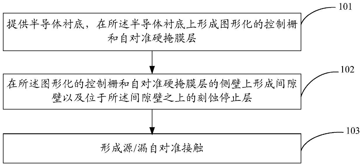
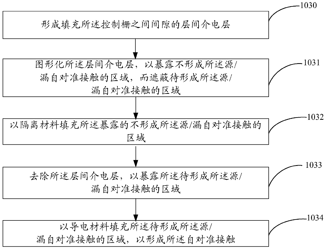
[0042] The following will refer to Figure 2A ~ Figure 2N as well as Figure 3A ~ Figure 3H A method for manufacturing a semiconductor device according to an embodiment of the present invention is described in detail, wherein, Figure 2A ~ Figure 2N It shows a schematic cross-sectional view in the direction of the active region of the semiconductor device obtained by sequentially implementing each step of the manufacturing method of the semiconductor device according to an embodiment of the present invention; Figure 3A ~ Figure 3H A schematic cross-sectional view of the active region direction and the isolation region direction of the semiconductor device obtained by sequentially implementing various steps in the method for manufacturing a semiconductor device according to an embodiment of the present invention is shown. in Figure 3A ~ Figure 3H corresponds to Figure 2G to Figure 2N ,and Figure 2A ~ Figure 2F Corresponding cross-sectional view of the isolation zone dir...

Embodiment 2

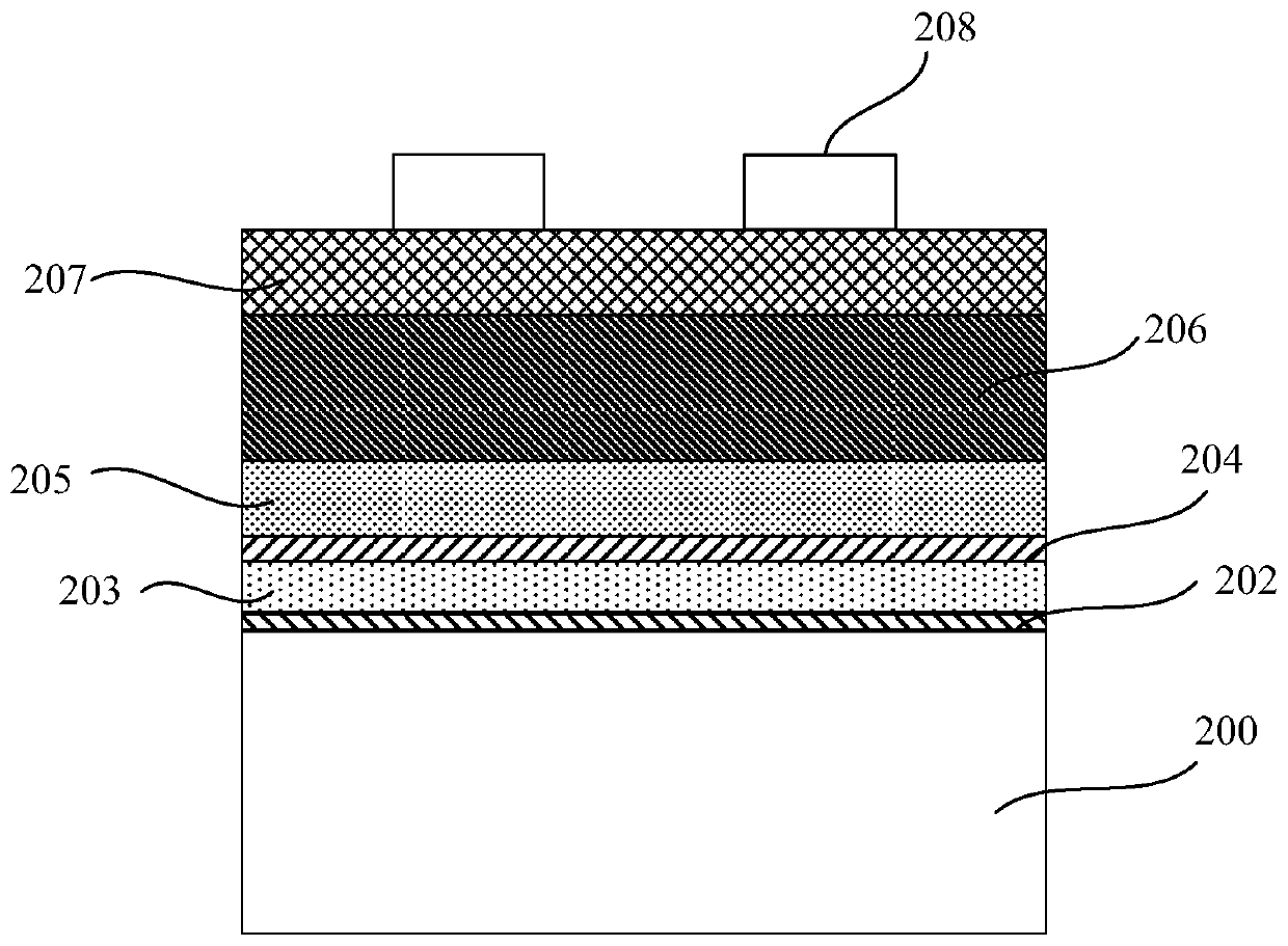
[0088] The present invention also provides a semiconductor device fabricated by the above method, such as Figure 4A with Figure 4BAs shown, the semiconductor device includes: a semiconductor substrate 400, an isolation structure 401 is formed in the semiconductor substrate 400, an active region is separated and defined by the isolation structure 401, and a gate stack is formed in the active region, so The gate stack includes a tunnel oxide layer 402, a floating gate 403, a gate dielectric layer 404, a control gate 405 and a hard mask layer 406, and the gate dielectric layer 404, the control gate 405 and a hard mask layer 406, a first spacer 407 and a second spacer 408 are formed on the sidewall of the gate stack and / or the sidewall of the control gate 405, A source / drain is formed on the side of the source / drain, and a self-aligned contact 409 located above the source and drain, and an isolation layer 410 is formed in a region outside the self-aligned contact 409 to isolate...

Embodiment 3

[0096] Still another embodiment of the present invention provides an electronic device, including a semiconductor device and an electronic component connected to the semiconductor device. Wherein, the semiconductor device includes: a semiconductor substrate, an isolation structure is formed in the semiconductor substrate, an active area is separated and defined by the isolation structure, a gate stack is formed in the active area, and the gate stack Including a tunnel oxide layer, a floating gate, a gate dielectric layer, a control gate and a hard mask layer, a gate dielectric layer, a control gate and a hard mask layer are formed on the isolation structure, and the gate A first spacer and a second spacer are formed on the sidewall of the stacked layer and / or the sidewall of the control gate, and source / drain electrodes are formed on both sides of the gate stack layer, and are located between the source and drain electrodes. self-aligned contacts on the self-aligned contacts, ...


PUM


Abstract

The invention provides a semiconductor device, a manufacturing method thereof, and an electronic device. The manufacturing method includes the following steps: providing a semiconductor substrate, forming a patterned control gate and a self-aligned hard mask layer on the semiconductor substrate; A spacer and an etch stop layer above the spacer are formed on the sidewalls of the patterned control gate and the self-aligned hard mask layer; source / drain self-aligned contacts are formed, wherein the patterned self-aligned hard mask The film layer includes a first portion and a second portion located below the first portion, the width of the first portion is smaller than the width of the second portion, and the spacer includes a side of the first portion of the self-aligned hard mask layer The first spacer on the wall and the second spacer are located on the second part of the self-aligned hard mask layer and the sidewall of the control gate, and the second spacer is completely wrapped by the etching stop layer. The manufacturing method can control the short circuit or breakdown of the gate and the source / drain in the NOR memory. The semiconductor device and electronic device have similar advantages.

Description

technical field [0001] The present invention relates to the technical field of semiconductors, in particular to a semiconductor device, a manufacturing method thereof, and an electronic device. Background technique [0002] With the development of semiconductor manufacturing technology, flash memory (flash memory) with faster access speed has been developed in terms of storage devices. Flash memory has the characteristics that information can be stored, read, and erased multiple times, and the stored information will not disappear after power failure. Therefore, flash memory has become a popular choice for personal computers and electronic devices. A widely used type of non-volatile memory. NOR ("NOR" electronic logic gate) type flash memory can be read or programmed in a random access manner, and due to its non-volatility (non-volatility), durability (durability) and Fast access time is widely used in mobile devices. [0003] For NOR flash memory, the source and drain co...

Claims


Application Information

Patent Timeline
Patent Type & Authority Patents(China)
IPC IPC(8): H01L27/11517H10B41/00
CPCH10B41/00
Inventor 王成诚李绍彬仇圣棻
Owner SEMICON MFG INT (SHANGHAI) CORP
Features
  • R&D
  • Intellectual Property
  • Life Sciences
  • Materials
  • Tech Scout
  • Unparalleled Data Quality
  • Higher Quality Content
  • 60% Fewer Hallucinations
Learn More