An integrated process method for norflash devices without cldd mask

A process method and device technology, applied in the field of semiconductor integrated circuit manufacturing

Active Publication Date: 2020-07-31
SHANGHAI HUALI MICROELECTRONICS CORP
View PDF6 Cites 0 Cited by
  • Summary
  • Abstract
  • Description
  • Claims
  • Application Information

AI Technical Summary

Problems solved by technology

The prior art Nor Flash device integration process requires three photolithography processes

Method used


Image

  • An integrated process method for norflash devices without cldd mask
  • An integrated process method for norflash devices without cldd mask
  • An integrated process method for norflash devices without cldd mask

Examples


Embodiment Construction

[0027] The specific embodiments of the present invention are given below in conjunction with the accompanying drawings, but the present invention is not limited to the following embodiments. Advantages and features of the present invention will be apparent from the following description and claims. It should be noted that all the drawings are in very simplified form and use imprecise ratios, which are only used for the purpose of conveniently and clearly assisting in describing the embodiments of the present invention.

[0028] The present invention proposes a kind of NorFlash device integration technique method that saves CLDD photomask, comprises the following steps:

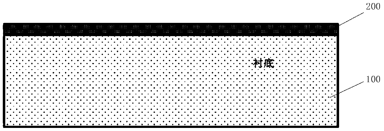
[0029] A tunnel oxide layer 200 is formed on the substrate 100, such as figure 1 shown;

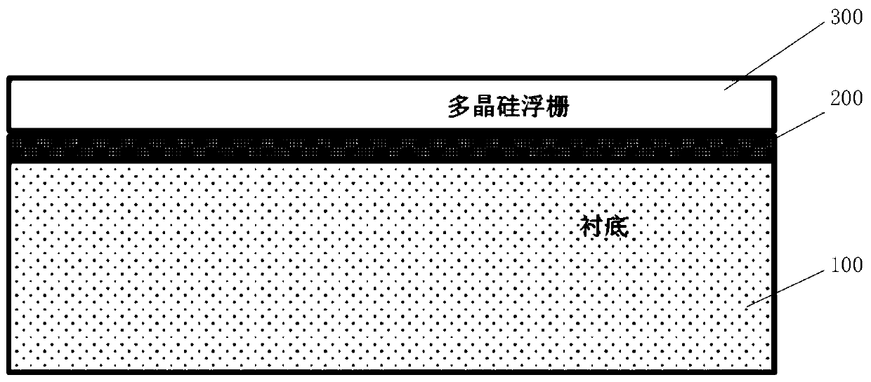
[0030] A polysilicon floating gate layer 300 is formed on the above structure, such as figure 2 shown;

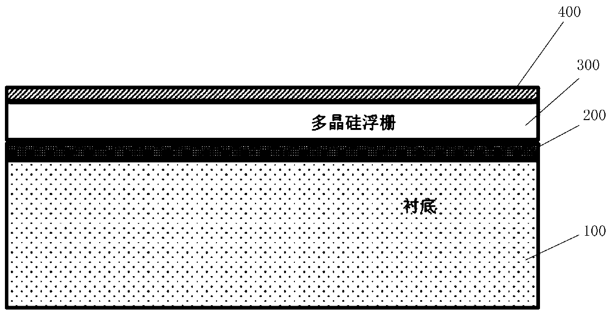
[0031] A dielectric layer 400 is formed on the above structure, such as image 3 shown;

[0032] A polysilic...


PUM

PropertyMeasurementUnit
thicknessaaaaaaaaaa
thicknessaaaaaaaaaa
thicknessaaaaaaaaaa

Abstract

The present invention proposes a kind of NorFlash device integration technique method that saves CLDD photomask, comprises the following steps: Forming tunnel oxide layer on substrate; Forming polysilicon floating gate layer; Forming medium layer; Forming polysilicon control gate layer; Resist layer, define the photoresist pattern, use dry etching to form the gate structure, remove the photoresist, perform ion implantation to form the light doped diffusion area of ​​the Flash device; coat the photoresist layer, define the photoresist pattern, Remove the photoresist above the source of the Flash device, perform ion implantation to form the source of the Flash device, and perform ion implantation again to compensate for the increase in source resistance caused by etching the source in the self-aligned source process; remove the photoresist to form The sidewall of the gate structure of the Flash device; perform ion implantation to form a heavily doped drain region of the Flash device. The invention can save the Nor Flash device integration process method of the CLDD photomask under the condition of not affecting the device performance, so as to achieve the purpose of reducing the process cost.

Description

technical field [0001] The invention relates to the field of semiconductor integrated circuit manufacturing, and in particular to a NorFlash device integration process method without CLDD mask. Background technique [0002] NOR flash memory is developed based on the ETOX structure proposed by Intel Corporation. It is a non-volatile memory, that is, the stored data can still be kept without loss after the chip is powered off. At the same time, NOR flash memory is a voltage-controlled device that uses hot electron injection to write data and erases data based on the tunnel effect. One of its notable features is its fast random read speed. [0003] As a non-volatile memory, NOR flash memory has the characteristics of non-volatility, high device density, low power consumption, and electrical rewritability. It is widely used in portable electronic products such as mobile phones, digital cameras, and smart cards. [0004] The Flash memory cell structure is similar to that of a MO...

Claims


Application Information

Patent Timeline
Patent Type & Authority Patents(China)
IPC IPC(8): H01L27/11524
CPCH10B41/35
Inventor 曹汝楠李娟娟王奇伟陈昊瑜
Owner SHANGHAI HUALI MICROELECTRONICS CORP
Why Eureka
Try Eureka