Double-selection conductive type dual-bracket grid-controlled source-drain variable resistance transistor and manufacturing method thereof

A conductivity type, transistor technology, applied in semiconductor/solid-state device manufacturing, transistors, semiconductor devices, etc., can solve the problems of gate loss of control, inability to change conductivity type, conductivity type cannot be switched, etc.

Active Publication Date: 2018-03-30
宿松新驱光电科技有限公司
View PDF3 Cites 0 Cited by
  • Summary
  • Abstract
  • Description
  • Claims
  • Application Information

AI Technical Summary

Problems solved by technology

However, in order to realize the switching characteristics of the gate electrode of the usual Schottky barrier field effect transistor (the gate electrode is forward-conducting and reverse-blocking or reverse-conducting and forward-blocking), it is necessary to perform a specific conductivity type on the source or drain region of the device. impurity doping, which makes it difficult to achieve a good Schottky contact between the source electrode and the source region, between the drain electrode and the drain region, and the doping of the source region and the drain region makes the gate electrode to the drain The control ability of the region and the source region is reduced, resulting in a decrease in the switching performance of the device
If the semiconductor region of the device is not doped, it is easy to realize the Schottky barrier between the source electrode and the source region, and the drain electrode and the drain region in the process, but this will cause the device to have different types in the forward and reverse directions. The carrier conduction of the gate electrode, that is, both the forward bias and reverse bias of the gate electrode will make the device in the conduction state, so that the gate loses its control function as the device switching device
[0004] In addition, based on the existing transistor technology, once the structure of the transistor is established, its conductivity type will also be established according to the conductivity type of the doped impurities. The transistors manufactured can only be P-type transistors or One of the N-type transistors whose conductivity type cannot be switched during operation
That is, during the working process of the transistor, its conductivity type cannot be changed by some control method

Method used


Image

  • Double-selection conductive type dual-bracket grid-controlled source-drain variable resistance transistor and manufacturing method thereof
  • Double-selection conductive type dual-bracket grid-controlled source-drain variable resistance transistor and manufacturing method thereof
  • Double-selection conductive type dual-bracket grid-controlled source-drain variable resistance transistor and manufacturing method thereof

Examples


Embodiment Construction

[0061] Below in conjunction with accompanying drawing, the present invention will be further described:

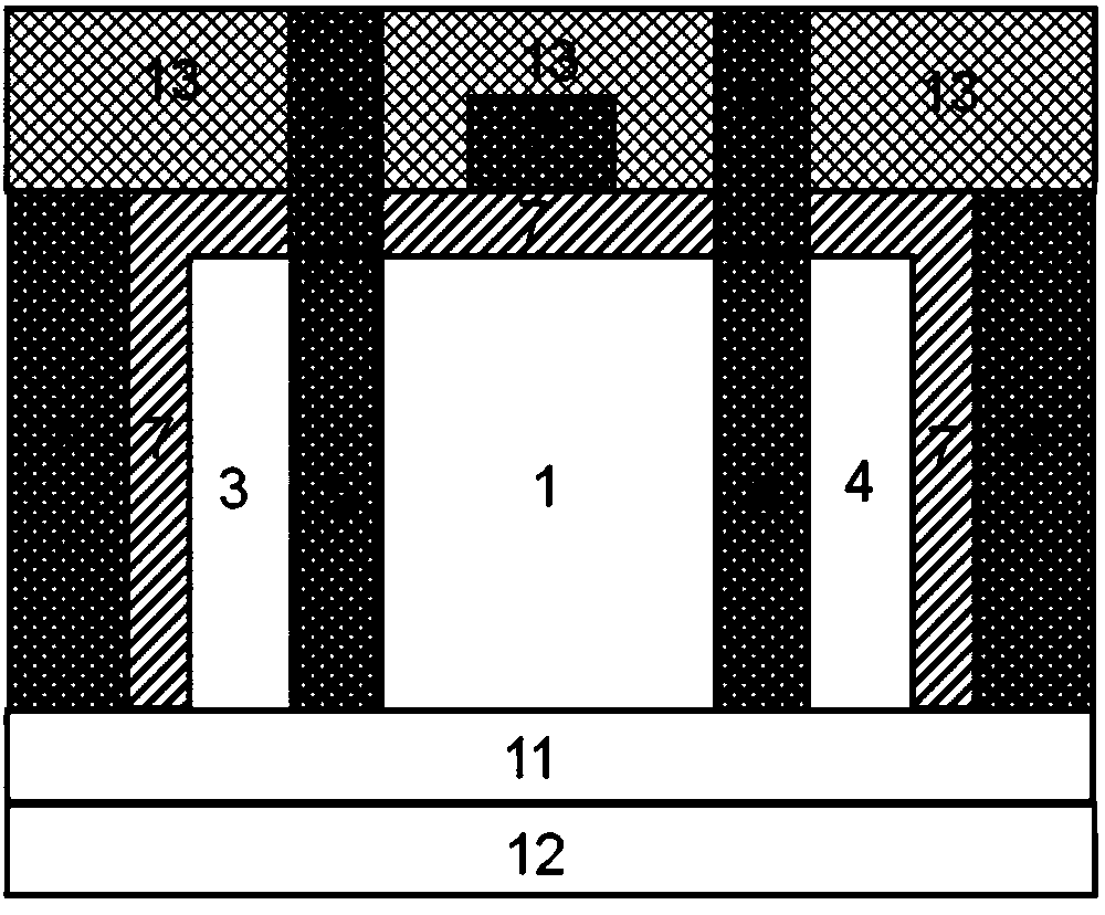
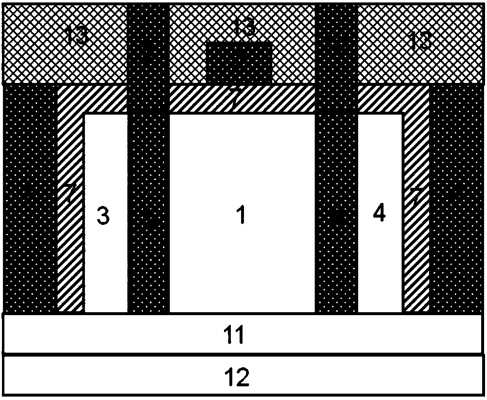
[0062] Such as figure 1 , figure 2 , image 3 and Figure 4 As shown, the dual-selection conduction type double-bracket gate-controlled source-drain resistance variable transistor includes a silicon substrate 12 of an SOI wafer, and above the silicon substrate 12 of the SOI wafer is a substrate insulating layer 11 of the SOI wafer. Above the round insulating substrate layer 11 are monocrystalline silicon thin film 1, part of folded auxiliary gate 2, source-drain interchangeable intrinsic region a3, source-drain interchangeable intrinsic region b4, metal source-drain interchangeable interchangeable region a5, metal source-drain interchangeable region b6, part of the gate electrode insulating layer 7, double-bracket gate electrode 8 and part of the insulating dielectric barrier layer 13; the single crystal silicon thin film 1 has an impurity concentration lower than 10 ...


PUM


Abstract

The invention relates to a double-selection conductive type dual-bracket grid-controlled source-drain variable resistance transistor and a manufacturing method thereof. The device has structural characteristics of folded auxiliary grid, dual-bracket grid and a left side and a right side which are symmetric to each other, the function that a P conductive type and an N conductive type can be freelyswitched can be achieved, and the transistor has the advantages of low static power consumption, low reverse leakage current, relatively high grid control capability and low sub-threshold amplitude. Compared with a conventional MOSFETs device, the transistor has the advantages that more excellent switch characteristic is achieved by a tunneling effect; and compared with a conventional tunneling field-effect transistor, the transistor has the bidirectional switch characteristic which a source and a drain can be symmetric to each other and can be exchanged and which is not possessed by the conventional tunneling field-effect transistor, the function that the P conductive type and the N conductive type can be freely switched and that cannot be achieved by the prior art is achieved, thus, wider and more versatile logic functions are provided for an integrated circuit design unit, and the transistor is suitable for promotion and application.

Description

technical field [0001] The invention relates to the field of ultra-large-scale integrated circuit manufacturing, in particular to a double-bracket gate-controlled source-drain resistance variable transistor with double-selection conduction type and a manufacturing method suitable for low-power integrated circuit manufacturing. Background technique [0002] When ordinary tunneling field effect transistors are used as switching devices, the tunneling mechanism of carriers is used, which can make the subthreshold swing of ordinary tunneling field effect transistors better than the 60mV / dec limit of MOSFETs type devices. However, tunneling field effect transistors based on silicon-based materials have limited tunneling probability due to the limited band gap. Compared with MOSFETs, it is difficult to generate a conduction current of the same order. More seriously, the source and drain electrodes Doping with impurities of different conductivity types, the asymmetric structural ch...

Claims


Application Information

Patent Timeline
Patent Type & Authority Applications(China)
IPC IPC(8): H01L29/78H01L29/417H01L29/06H01L21/336
CPCH01L29/0603H01L29/41758H01L29/66477H01L29/66568H01L29/78618
Inventor 靳晓诗高云翔刘溪
Owner 宿松新驱光电科技有限公司
Why Eureka
Try Eureka