H-shaped gate-controlled source-drain resistance variable conduction type adjustable transistor and manufacturing method thereof

A conductivity type, source-drain technology, used in semiconductor/solid-state device manufacturing, semiconductor devices, circuits, etc., can solve problems such as inability to change the conductivity type, non-switchable conductivity types, and reduced gate electrode control of drain and source regions.

Active Publication Date: 2019-11-22
深圳市麦思浦半导体有限公司
View PDF2 Cites 0 Cited by
  • Summary
  • Abstract
  • Description
  • Claims
  • Application Information

AI Technical Summary

Problems solved by technology

However, in order to realize the switching characteristics of the gate electrode of the usual Schottky barrier field effect transistor (the gate electrode is forward-conducting and reverse-blocking or reverse-conducting and forward-blocking), it is necessary to perform a specific conductivity type on the source or drain region of the device. impurity doping, which makes it difficult to achieve a good Schottky contact between the source electrode and the source region, between the drain electrode and the drain region, and the doping of the source region and the drain region makes the gate electrode to the drain The control ability of the region and the source region is reduced, resulting in a decrease in the switching performance of the device
If the semiconductor region of the device is not doped, it is easy to realize the Schottky barrier between the source electrode and the source region, and the drain electrode and the drain region in the process, but this will cause the device to have different types in the forward and reverse directions. The carrier conduction of the gate electrode, that is, both the forward bias and reverse bias of the gate electrode will make the device in the conduction state, so that the gate loses its control function as the device switching device
[0004] In addition, based on the existing transistor technology, once the structure of the transistor is established, its conductivity type will also be established according to the conductivity type of the doped impurities. The transistors manufactured can only be P-type transistors or One of the N-type transistors whose conductivity type cannot be switched during operation
That is, during the working process of the transistor, its conductivity type cannot be changed by some control method

Method used


Image

  • H-shaped gate-controlled source-drain resistance variable conduction type adjustable transistor and manufacturing method thereof
  • H-shaped gate-controlled source-drain resistance variable conduction type adjustable transistor and manufacturing method thereof
  • H-shaped gate-controlled source-drain resistance variable conduction type adjustable transistor and manufacturing method thereof

Examples


Embodiment Construction

[0081] Below in conjunction with accompanying drawing, the present invention will be further described:

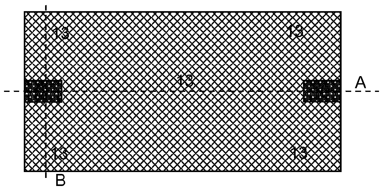
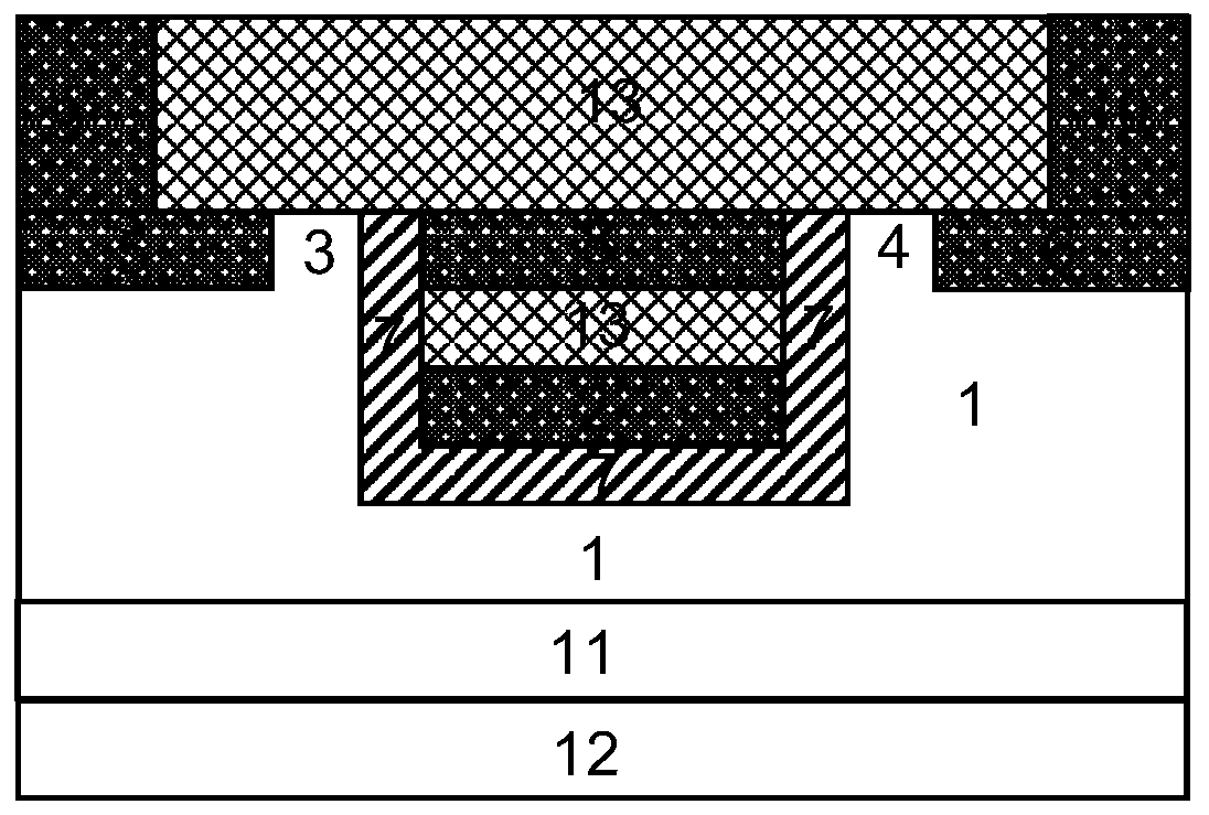
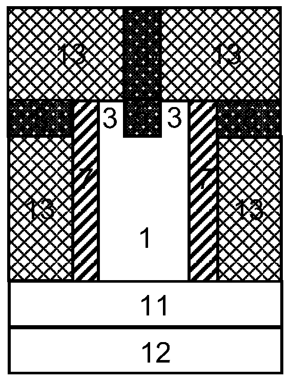
[0082] Such as figure 1 , figure 2 with image 3 As shown, an H-shaped gate-controlled source-drain resistance variable conduction type adjustable transistor includes a silicon substrate 12 of an SOI wafer, and above the silicon substrate 12 of the SOI wafer is a substrate insulating layer 11 of the SOI wafer. , above the substrate insulating layer 11 of the SOI wafer are the monocrystalline silicon film 1, the conductivity type control gate 2, the gate electrode insulating layer 7 and the partial area of ​​the insulating dielectric barrier layer 13, and the monocrystalline silicon film 1 has a "concave" shape Geometric features, impurity concentration below 10 16 cm -3The single crystal silicon semiconductor material, the inner surface of the groove-shaped structure formed by the single crystal silicon thin film 1 and the front and rear outer surfaces are attached wi...


PUM


Abstract

The invention relates to an H-shaped gate-controlled drain-source resistance-variable conductivity type adjustable transistor and a manufacturing method thereof. The transistor comprises an H-shaped gate electrode, a conductivity type regulation and control gate and a left-right symmetric structure characteristic. According to the invention, the free switching function between a P type conductivity type and an N type conductivity type, and the bidirectional switching function are realized. The advantages of low static power consumption, low reverse leakage current, strong gate control capability and low subthreshold swing are realized. Compared with a common MOSFET type device, the schottky barrier tunneling effect is utilized to achieve better subthreshold characteristics and switching characteristics. The static power consumption of the transistor is reduced. Compared with a common tunneling field effect transistor, the bidirectional switching characteristics, wherein a drain electrode and a source electrode are symmetrical and interchangeable, can be realized, wherein the bidirectional switching characteristics cannot be realized by the common tunneling field effect transistor.The free regulation and control function of the P type conductivity type and the N type conductivity type, which cannot be realized by various existing transistor technologies, can be realized. Therefore, the H-shaped gate-controlled drain-source resistance-variable conductivity type adjustable transistor is suitable for popularization and application.

Description

technical field [0001] The invention relates to the field of ultra-large-scale integrated circuit manufacturing, in particular to an H-shaped gate-controlled source-drain resistance variable conduction type adjustable transistor with low leakage current suitable for low-power integrated circuit manufacturing and a manufacturing method thereof. Background technique [0002] When ordinary tunneling field effect transistors are used as switching devices, they use the tunneling mechanism of carriers, which can make the subthreshold swing of ordinary tunneling field effect transistors better than the 60mV / dec limit of MOSFETs. However, tunneling field effect transistors based on silicon-based materials have limited tunneling probability due to the limited band gap. Compared with MOSFETs, it is difficult to generate a conduction current of the same order. More seriously, the source and drain electrodes Doping with impurities of different conductivity types, the asymmetric structur...

Claims


Application Information

Patent Timeline
Patent Type & Authority Patents(China)
IPC IPC(8): H01L29/08H01L29/423H01L29/78H01L21/336H01L21/28
CPCH01L29/0847H01L29/42356H01L29/66643H01L29/7839
Inventor 靳晓诗高云翔刘溪
Owner 深圳市麦思浦半导体有限公司
Why Eureka
Try Eureka