A kind of oled device structure and preparation method
A device structure and thin film technology, which is applied in semiconductor/solid-state device manufacturing, semiconductor devices, and electric solid-state devices, etc., can solve the problems of affecting the light transmittance of the device, poor barrier performance, and reducing the light extraction efficiency of the device, so as to improve the light extraction efficiency. , The production method is simple, and the effect of increasing the light output efficiency
- Summary
- Abstract
- Description
- Claims
- Application Information
AI Technical Summary
Problems solved by technology
Method used
Image
Examples
Embodiment 1
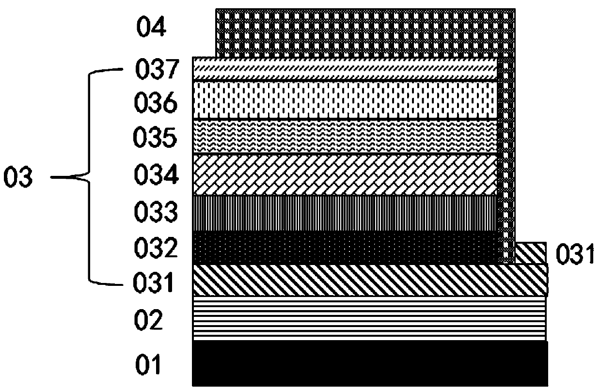
[0040] like figure 1 As shown, an OLED device structure is suitable for bottom-emitting OLED devices, including:
[0041] A substrate 01, the substrate 01 comprising a glass substrate or a polymer substrate;
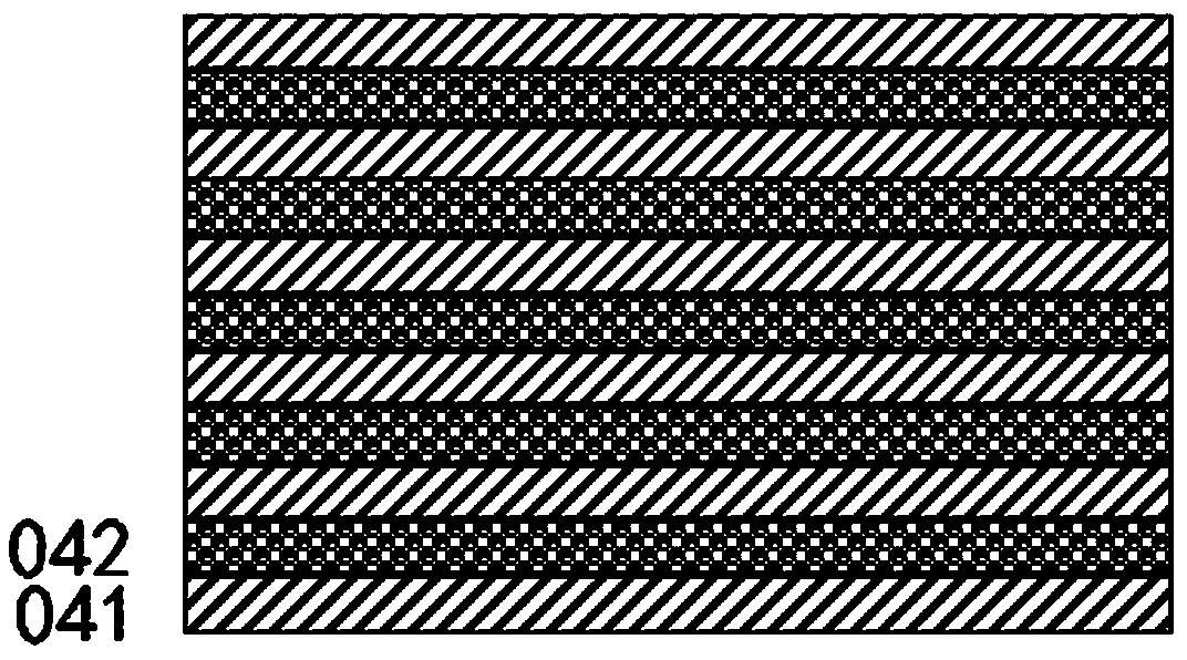
[0042] The first water-oxygen barrier layer 02 with high light transmittance is arranged on the substrate 01, such as figure 2As shown, the first water-oxygen barrier layer 02 is alternately formed by the first low-refractive index film 021 and the first high-refractive index film 022 from bottom to top according to the number of alternating cycles m+0.5, m takes a positive integer, and 0.5 represents The topmost layer of the first water-oxygen barrier layer 02 is the first low-refractive index film 021, that is, an additional layer of low-refractive index film is coated on the film layer to form a low / high / low sandwich structure. The first low-refractive index film 021 The refractive index is smaller than the refractive index of the first high refractive index film 0...
Embodiment 2
[0073] The difference between this embodiment and Embodiment 1 is that the positions of the first water-oxygen barrier layer 02 and the second water-oxygen barrier layer 04 are reversed in the structure of the OLED device, and a second water-oxygen barrier layer with high optical reflectivity is arranged above the substrate 01. Oxygen barrier layer 04, the first water and oxygen barrier layer 02 with high light transmittance is arranged on the OLED unit 03, which is suitable for top-emitting OLED devices. The specific structure is:
[0074] The cross-sections of the second water-oxygen barrier layer 04 and the anode 031 are L-shaped, the short side of the second water-oxygen barrier layer 04 is located on the electron injection layer 036, and the long side of the second water-oxygen barrier layer 04 is vertically downward and The long-side inner wall of the second water-oxygen barrier layer 04 is close to the vertical end faces of the hole injection layer 032, the hole transpo...
PUM
 Abstract
Description
Claims
Application Information


