Lateral double diffused metal oxide semiconductor field effect transistor with potential floating field plate

An oxide semiconductor and lateral double-diffusion technology, which is applied in the direction of semiconductor devices, circuits, electrical components, etc., can solve the problems of inability to uniform surface electric field distribution of devices, inability to adjust device current capacity, etc.

Active Publication Date: 2020-09-04
UNIV OF JINAN
View PDF4 Cites 0 Cited by
  • Summary
  • Abstract
  • Description
  • Claims
  • Application Information

AI Technical Summary

Problems solved by technology

Field plate technology is an effective means to optimize the surface electric field of LDMOS devices, but the traditional field plate technology cannot make the device obtain a uniform surface electric field distribution, and there is still room for improvement
At the same time, the potential of the traditional field plate is fixed at a low potential, so that the traditional field plate only works when the device is in the off-voltage withstand state, but cannot adjust the current capability of the device in the on-state

Method used


Image

  • Lateral double diffused metal oxide semiconductor field effect transistor with potential floating field plate
  • Lateral double diffused metal oxide semiconductor field effect transistor with potential floating field plate

Examples


Embodiment Construction

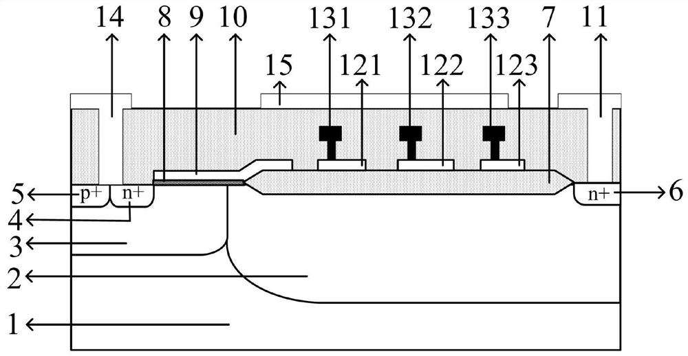
[0020] refer to figure 1 , a lateral double-diffused metal oxide semiconductor field effect transistor with a potential floating type field plate, comprising: a P-type semiconductor substrate 1, an N-type drift region 2 and a P-type well 3 are arranged on the P-type semiconductor substrate 1, An N-type source region 4 and a P-type contact region 5 are arranged on the P-type well 3, an N-type drain region 6 and a field oxide layer 7 are arranged on the N-type drift region 2, and a part of the N-type drift region 2 and a part of the P-type A gate oxide layer 8 is arranged above the type well 3, and one end of the gate oxide layer 8 is against the boundary of the N-type source region 4, and the other end of the gate oxide layer 8 is against the boundary of the field oxide layer 7. In the gate oxide layer 8 is provided with a polysilicon gate 9, and the polysilicon gate 9 extends to the top of the field oxide layer 7, in part of the P-type well 3, the P-type contact region 5, the...


PUM


Abstract

The invention discloses an N-type lateral double-diffused metal oxide semiconductor field effect transistor with a charge-adjustable field plate, comprising: a P-type semiconductor substrate, on which an N-type drift region and a P-type semiconductor substrate are arranged. type well, an N-type source region, a P-type contact region, and a gate oxide layer are arranged on the P-type well, and an N-type drain region and a field oxide layer are arranged on the N-type drift region, and it is characterized in that the field oxide layer There are multiple charge-adjustable field plates on the surface, and each charge-adjustable field plate is connected with a metal induction layer, and a source metal is connected to the P-type contact area and the N-type source area, and the source metal Completely cover all metal sensing layers. This structure can obtain a uniform surface lateral electric field distribution in the entire drift region of the device, has a high lateral withstand voltage capability, and can increase the doping concentration of the drift region of the device while maintaining a high breakdown voltage, thereby obtaining low conduction resistance.

Description

technical field [0001] The present invention relates to the field of power semiconductor devices, more specifically, it relates to a lateral double-diffused metal oxide semiconductor field effect transistor (LDMOS) suitable for high-voltage applications, which is suitable for high-voltage, low-current applications such as printers, motors, and flat panel displays. Field driver chip. Background technique [0002] A lateral double diffused metal oxide semiconductor transistor (LDMOS) is a lateral high voltage device of a double diffused metal oxide semiconductor transistor device (DMOS). It has the advantages of high withstand voltage, large gain, low distortion, etc., and is more compatible with CMOS technology, so it is widely used in intelligent power integrated circuits. At present, the design focus of the lateral double-diffused metal-oxide-semiconductor transistor (LDMOS) is how to reasonably alleviate the contradiction between the breakdown voltage and the on-resistanc...

Claims


Application Information

Patent Timeline
Patent Type & Authority Patents(China)
IPC IPC(8): H01L29/40H01L29/78
CPCH01L29/404H01L29/7816H01L29/7835H01L29/42368
Inventor 张春伟李志明李阳李威岳文静付小倩王靖博
Owner UNIV OF JINAN
Why Eureka
Try Eureka