GaN based monolithic power inverter and manufacturing method thereof

A power inverter, monolithic technology, applied in the direction of converting AC power input to DC power output, output power conversion device, semiconductor/solid-state device manufacturing, etc., can solve the constraints of high performance and process difficulty of GaN-based power integrated circuits Large and other problems, to achieve the effect of reducing the difficulty of production, simplifying the production process, and improving the yield of devices

Active Publication Date: 2018-04-06
INST OF MICROELECTRONICS CHINESE ACAD OF SCI
View PDF6 Cites 7 Cited by
  • Summary
  • Abstract
  • Description
  • Claims
  • Application Information

AI Technical Summary

Problems solved by technology

However, it is very difficult to realize high-performance enhancement mode and depletion mode GaN-based power diodes on the same substrate at the same time, which restricts the development of GaN-based power integrated circuits in the direction of high-efficiency, small and intelligent applications.

Method used


Image

  • GaN based monolithic power inverter and manufacturing method thereof
  • GaN based monolithic power inverter and manufacturing method thereof
  • GaN based monolithic power inverter and manufacturing method thereof

Examples


Embodiment Construction

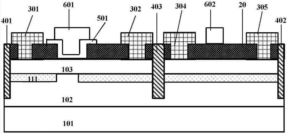
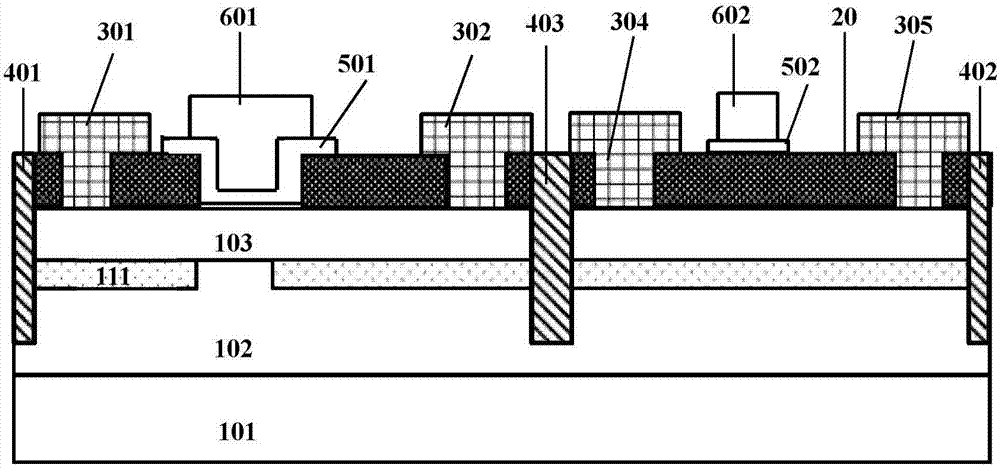
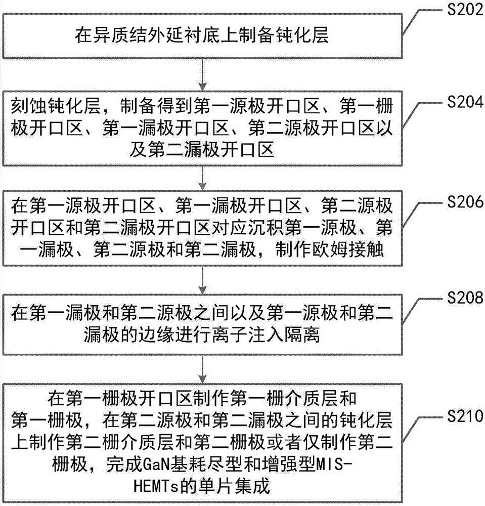
[0039] The present disclosure provides a GaN-based monolithic power inverter and a manufacturing method thereof. By adopting an ultra-thin barrier Al(In,Ga)N / GaN heterojunction epitaxial substrate, polycrystalline SiN, SiO are deposited on it 2 , SiON passivation layer, no need to etch Al(In,Ga)N barrier layer, GaN-based depletion mode and enhanced metal insulating layer semiconductor high electron mobility transistors (MIS-HEMTs, metal-insulator-semiconductor high -electron-mobility transistors) monolithic integration and manufacturing; as a whole, the industrialized preparation and monolithic integration of GaN-based enhancement mode and depletion mode power transistors are realized, which strongly promotes GaN power integrated circuits toward high-efficiency, small and compact Direction development.

[0040] In order to make the objectives, technical solutions, and advantages of the present disclosure clearer, the following further describes the present disclosure in detail wit...


PUM


Abstract

The present invention discloses a GaN based monolithic power inverter and a manufacturing method thereof. The power inverter comprises: a heterojunction epitaxial substrate; passivation layers formedon the heterojunction epitaxial substrate and provided with a plurality of hollow areas between the passivation layers; a normally OFF power triode structure formed in the hollow areas in the plurality of the hollow areas and comprising a first source electrode, a first drain electrode and a first grid electrode, wherein the first source electrode and the first drain electrode both achieve Ohmic contact with a thin barrier layer, and the first grid electrode and the thin barrier layer achieve insulation through a first gate dielectric layer located at the lower portion the first grid electrode; and an normally ON power triode structure formed at the other hollow areas in the plurality of hollow areas and comprising a second source electrode, a second drain electrode and a second grid electrode, wherein the second source electrode and the second drain electrode both achieve Ohmic contact with the thin barrier layer, and the second grid electrode and the passivation layers achieve insulation through a second gate dielectric layer located at the lower portion the second grid electrode or the second grid electrode is in direct contact with the passivation layers. The preparation technology of the power converter is simple, the structure is diversified, and the device yield is improved.

Description

Technical field [0001] The present disclosure belongs to the technical field of semiconductor devices, and relates to a GaN-based monolithic power inverter and a manufacturing method thereof. Background technique [0002] The power inverter (power inverter) composed of cascaded power transistors of enhanced (normally OFF) and depleted (normall ON) power transistors is the basic unit of the inverter circuit and is applied to various DC / AC conversion modules. However, it is currently difficult to achieve high-performance enhanced and depleted GaN-based power diodes on the same substrate at the same time, which restricts the development of GaN-based power integrated circuits to high-efficiency, small-scale and intelligent applications. Therefore, there is an urgent need to provide a new monolithic integrated power inverter and manufacturing method that can realize both enhancement mode and depletion mode on the same substrate, and the manufacturing process is simple and convenient, ...

Claims


Application Information

Patent Timeline
Patent Type & Authority Applications(China)
IPC IPC(8): H01L27/06H01L29/423H01L29/778H01L21/8252H02M7/00
CPCH01L21/8252H01L27/0623H01L29/42364H01L29/7787H02M7/003Y02B70/10
Inventor 黄森刘新宇王鑫华康玄武魏珂
Owner INST OF MICROELECTRONICS CHINESE ACAD OF SCI
Why Eureka
Try Eureka