Semiconductor structure and forming method therefor

A technology of semiconductor and gate structure, applied in the field of semiconductor structure and its formation, can solve the problem that the electrical performance of semiconductor devices needs to be improved, etc.

Active Publication Date: 2018-04-17
SEMICON MFG INT (SHANGHAI) CORP +1
View PDF12 Cites 3 Cited by
  • Summary
  • Abstract
  • Description
  • Claims
  • Application Information

AI Technical Summary

Problems solved by technology

[0004] Although the introduction of high-k metal gates can improve the electrical performance of semiconductor devices to a certain extent, the electrical performance of semiconductor devices formed by the prior art still needs to be improved.

Method used


Image

  • Semiconductor structure and forming method therefor
  • Semiconductor structure and forming method therefor
  • Semiconductor structure and forming method therefor

Examples


Embodiment Construction

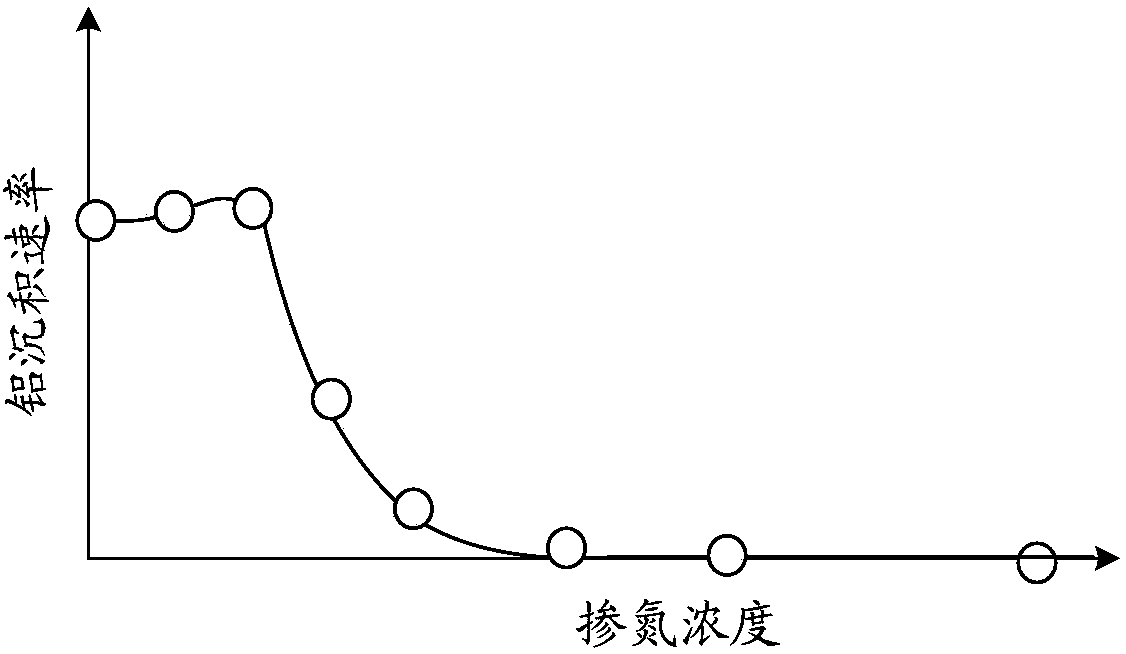
[0033] It can be seen from the background art that the electrical performance of semiconductor devices still needs to be improved. Combined with a method of forming a semiconductor structure, the reason is analyzed.

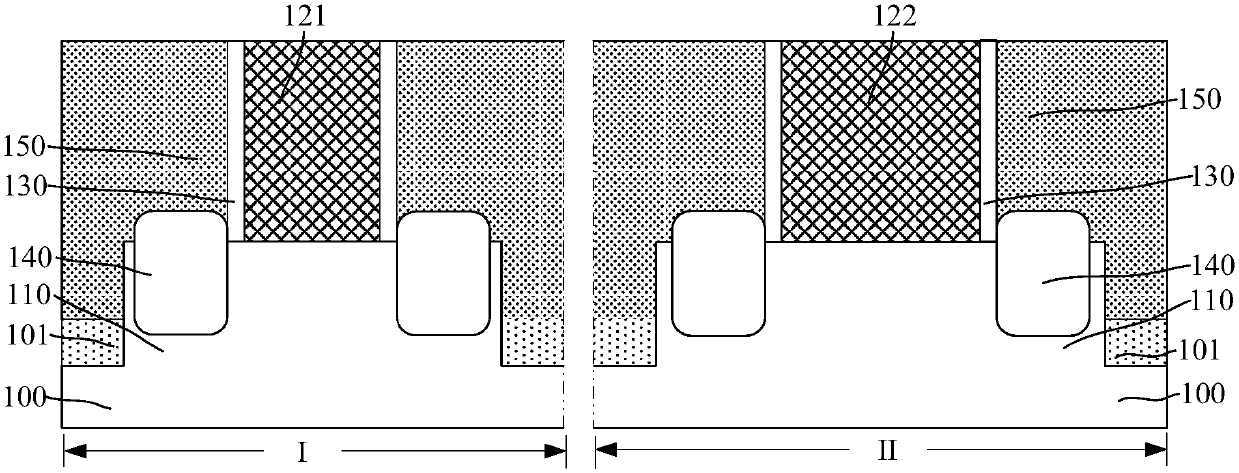
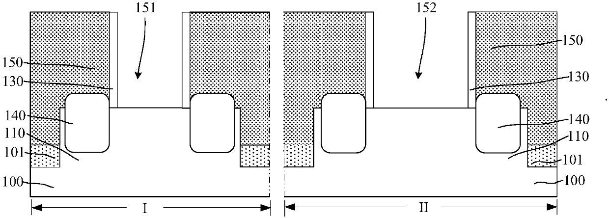
[0034] The forming method includes: providing a substrate, the substrate includes a first region for forming a first transistor and a second region for forming a second transistor, the length of a channel region of the first transistor is smaller than that of the second transistor. The length of the channel region of the transistor; an interlayer dielectric layer is formed on the substrate; a first opening exposing the substrate of the first region and a second opening exposing the substrate of the second region are formed in the interlayer dielectric layer ; forming a gate dielectric layer on the bottom and sidewalls of the first opening and on the bottom and sidewalls of the second opening; forming a work function layer on the gate dielectric layer; The metal ...


PUM


Abstract

The invention provides a semiconductor structure and a forming method therefor, and the method comprises the steps: providing a substrate which comprises a first region for forming a first transistorand a second region for forming a second transistor, wherein the trench length of the first transistor is less than the trench length of the second transistor; forming an interlayer dielectric layer on the substrate; forming a first opening and a second opening in the interlayer dielectric layer; forming gate medium layers on the bottom and side walls of a first opening and the bottom and side walls of the second opening; forming a first nitrogenous layer on a gate medium layer of the second region; and forming work function layers containing aluminium on the gate medium layer of the first region and the first nitrogenous layer. According to the invention, the first nitrogenous layer is formed, thereby reducing the deposition capability of aluminium atoms in the second opening, so as to solve a problem that the inconsistency of the longitudinal width ratios of the openings causes the inconsistency of the deposition capability of aluminium atoms, enable the thickness values of the workfunction layers of the first and second transistors to be approximately equal and enable the aluminium contents to be approximately equal.

Description

technical field [0001] The invention relates to the field of semiconductors, in particular to a semiconductor structure and a forming method thereof. Background technique [0002] The main semiconductor device of an integrated circuit, especially a very large scale integrated circuit, is a metal-oxide-semiconductor field effect transistor (MOS transistor). With the continuous development of integrated circuit manufacturing technology, the technology nodes of semiconductor devices continue to decrease, and the geometric dimensions of semiconductor devices follow Moore's law. When the size of semiconductor devices is reduced to a certain extent, various secondary effects caused by the physical limits of semiconductor devices appear one after another, and it becomes more and more difficult to scale down the feature size of semiconductor devices. Among them, in the field of semiconductor manufacturing, the most challenging thing is how to solve the problem of large leakage curr...

Claims


Application Information

Patent Timeline
Patent Type & Authority Applications(China)
IPC IPC(8): H01L21/8234H01L27/088H01L29/51
CPCH01L21/823462H01L27/088H01L29/518
Inventor 徐建华邓浩
Owner SEMICON MFG INT (SHANGHAI) CORP
Why Eureka
Try Eureka