Semiconductor device, manufacturing method thereof and electronic device
A manufacturing method and semiconductor technology, which are applied in semiconductor/solid-state device manufacturing, semiconductor devices, electric solid-state devices, etc., can solve problems such as unfavorable short-channel effect and poor lateral phosphorus diffusion ability, and achieve good short-channel effect and improve Performance and yield, the effect of large contact area
- Summary
- Abstract
- Description
- Claims
- Application Information
AI Technical Summary
Problems solved by technology
Method used
Image

Examples
Embodiment 1
[0074] In view of the problems existing in the prior art, the present invention provides a method for manufacturing a semiconductor device, such as Figure 20 As shown, it mainly includes the following steps:
[0075] Step S201, providing a semiconductor substrate, the semiconductor substrate includes a PMOS region and an NMOS region, and a first fin structure and a second fin structure are respectively formed on the semiconductor substrate in the PMOS region and the NMOS region;
[0076] Step S202, forming a first dummy gate structure and a second dummy gate structure across a part of the first fin structure and a part of the second fin structure in the PMOS region and the NMOS region, respectively;
[0077] Step S203, growing a first stressed epitaxial layer in the source / drain regions of the first fin structure on both sides of the first dummy gate structure;
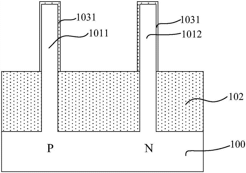
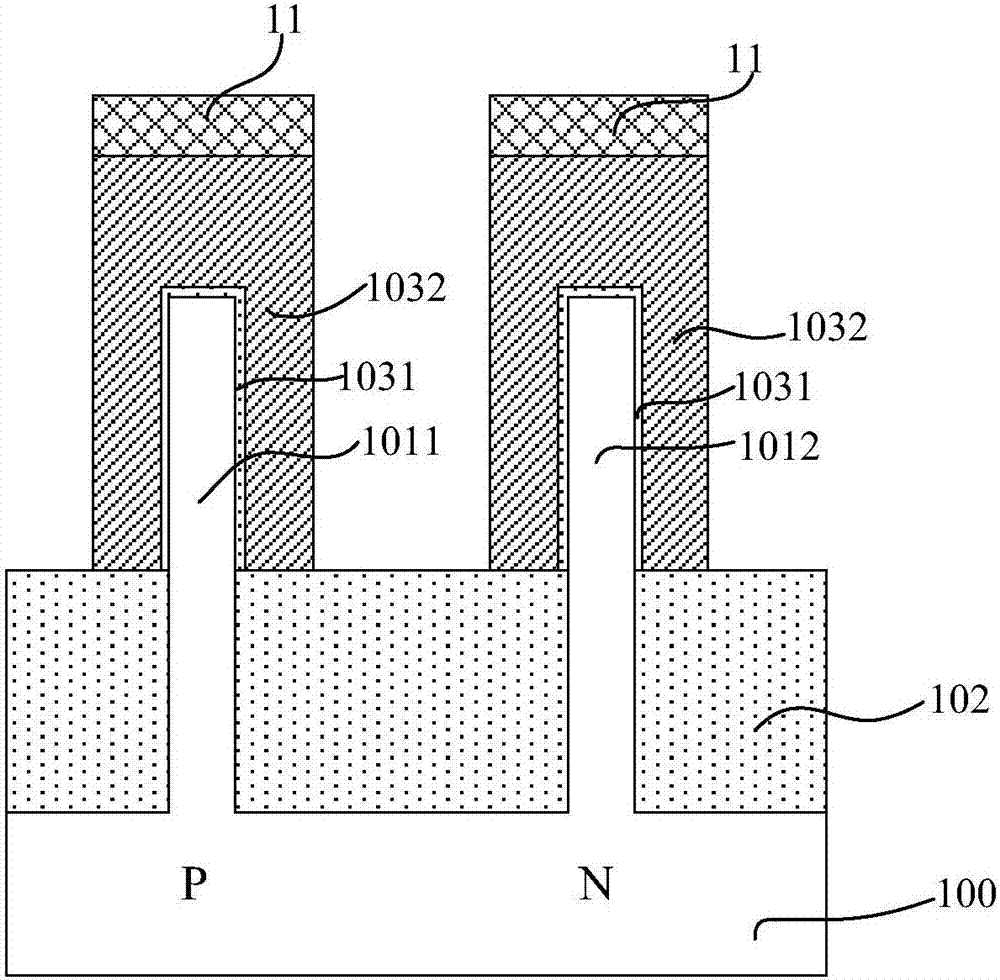
[0078] Step S204, forming first spacers on both side walls of the second fin structure on both sides of the secon...
Embodiment 2
[0190] The present invention also provides a semiconductor device prepared by using the method in the first embodiment above.
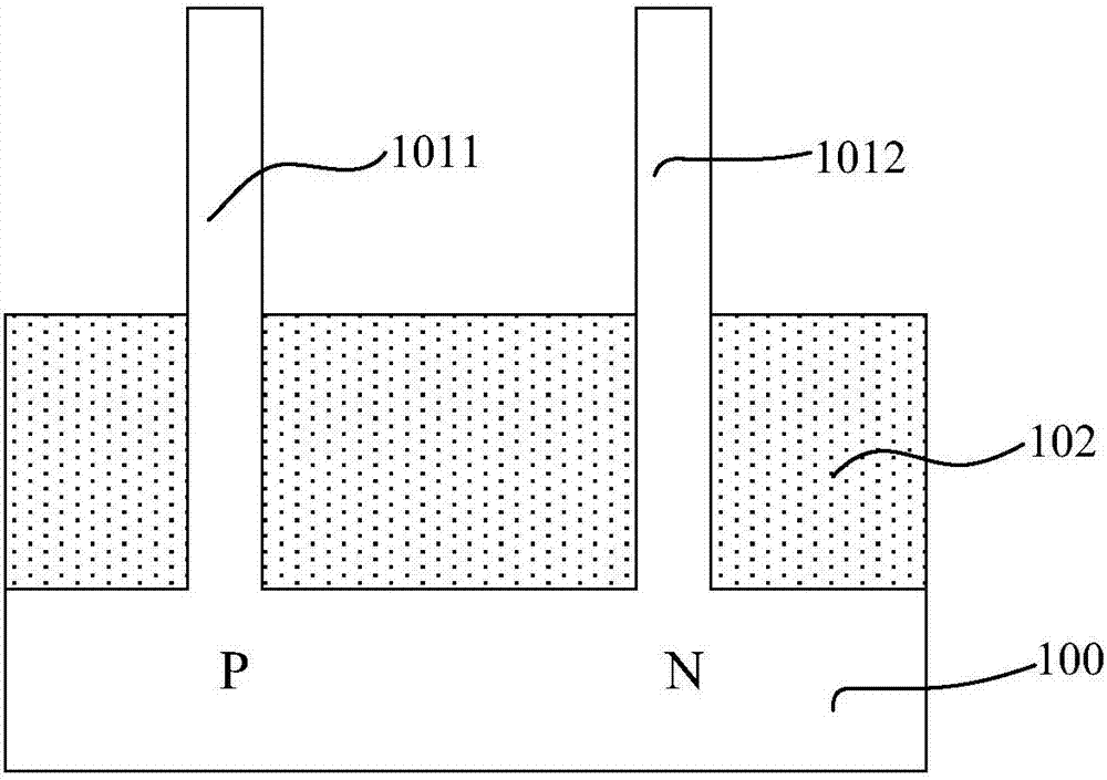
[0191] Specifically, as Figure 17 and Figure 18 As shown, the semiconductor device of the present invention includes a semiconductor substrate 100, the semiconductor substrate 100 includes a PMOS region and an NMOS region, and a first fin structure is respectively formed on the semiconductor substrate 100 in the PMOS region and the NMOS region 1011 and a second fin structure 1012 .
[0192] Specifically, the semiconductor substrate 100 may be at least one of the materials mentioned below: Si, Ge, SiGe, SiC, SiGeC, InAs, GaAs, InP or other III / V compound semiconductors, including these semiconductor components multi-layer structure, etc., or silicon-on-insulator (SOI), silicon-on-insulator (SSOI), silicon-germanium-on-insulator (S-SiGeOI), silicon-germanium-on-insulator (SiGeOI) and germanium-on-insulator (GeOI) wait. In this embodiment, the semi...
Embodiment 3
[0222] The present invention also provides an electronic device, including the semiconductor device described in the second embodiment, and the semiconductor device is prepared according to the method described in the first embodiment.
[0223] The electronic device of this embodiment can be any electronic device such as a mobile phone, a tablet computer, a notebook computer, a netbook, a game console, a TV set, a VCD, a DVD, a navigator, a digital photo frame, a camera, a video camera, a recording pen, MP3, MP4, PSP, etc. Product or equipment, but also any intermediate product including electrical circuits. The electronic device according to the embodiment of the present invention has better performance due to the use of the above-mentioned semiconductor device.
[0224] in, Figure 20 An example of a mobile phone handset is shown. The mobile phone handset 300 is provided with a display portion 302 included in a housing 301, operation buttons 303, an external connection por...
PUM
| Property | Measurement | Unit |
|---|---|---|
| Thickness | aaaaa | aaaaa |
| Thickness | aaaaa | aaaaa |
Abstract
Description
Claims
Application Information