

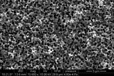
Polycrystalline black silicon wafer diffusion method through MCCE etching
A diffusion method, black silicon technology, applied in the field of solar cells, can solve the problems of difficult diffusion, poor square resistance uniformity, easy burn-through, etc., and achieve good electrical properties, good uniformity, and good effect
- Summary
- Abstract
- Description
- Claims
- Application Information
AI Technical Summary
Problems solved by technology
Method used
Image

Examples
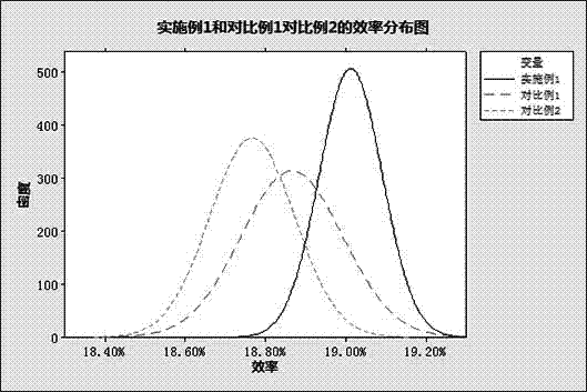
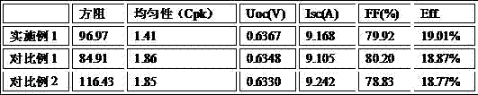
Embodiment 1
[0023] Example 1: An MCCE texturing polycrystalline black silicon wafer diffusion method, which is suitable for the black silicon diffusion process prepared by metal-catalyzed chemical etching:
[0024] In the first deposition process, the nitrogen flow rate of the phosphorus source is 600~800 sccm, the large nitrogen flow rate is 13.9slm, the oxygen flow rate is 1300 sccm, the temperature is 795 °C, and the deposition treatment time is 600s~700s;
[0025] In the first advancing process, the nitrogen flow of the phosphorus source is 0 sccm, the large nitrogen flow is 16 slm, the oxygen flow is 0 sccm, the temperature is 832 °C, and the advancing treatment time is 500s~600s;
[0026] In the second deposition process, the nitrogen flow rate of the phosphorus source is 1500~1700 sccm, the large nitrogen flow rate is 12.5 slm, the oxygen flow rate is 1900 sccm, the temperature is 832 °C, and the deposition treatment time is 300s~400s;
[0027] In the second advancing process, the nitrogen ...
PUM
 Abstract
Description
Claims
Application Information