Manufacture method of electrode, TFT (Thin Film Transistor) and manufacture method thereof and related substrate

A technology for thin film transistors and manufacturing methods, applied in the fields of array substrates, electrode manufacturing methods, thin film transistors and their manufacturing methods, and display devices, capable of solving problems such as low etching efficiency, complicated processes, and material waste, and reducing production costs Effect

Inactive Publication Date: 2018-05-11
BOE TECH GRP CO LTD +1
View PDF2 Cites 4 Cited by
  • Summary
  • Abstract
  • Description
  • Claims
  • Application Information

AI Technical Summary

Problems solved by technology

[0004] The existing technology generally adopts traditional photolithography technology or ion beam etching technology to realize the preparation of short-channel (channel length less than or equal to 5 microns) oxide thin film transistors. Although these technologies can effectively realize the preparation of short-channel oxide devices , but there are problems such as material waste, complicated process, high production cost, low etching efficiency, and inability to produce in large areas.

Method used


Image

  • Manufacture method of electrode, TFT (Thin Film Transistor) and manufacture method thereof and related substrate
  • Manufacture method of electrode, TFT (Thin Film Transistor) and manufacture method thereof and related substrate
  • Manufacture method of electrode, TFT (Thin Film Transistor) and manufacture method thereof and related substrate

Examples


Embodiment 1

[0096] The fabrication of short-channel inorganic semiconductor thin film transistors with a bottom-gate and top-contact structure will be described in detail below.

[0097] Such as Figure 9 As shown, the grid 220 is first fabricated on the substrate 100. The material of the grid 220 is metal or conductive oxide. The grid 220 can be fabricated by sputtering, evaporation, solution coating or printing. The specific details of the grid 220 The manufacturing method is similar to the prior art, and will not be repeated here.

[0098] Next, a gate insulating layer 230 is formed on the gate 220. The gate insulating layer 230 is a composition of a single-layer oxide or a multi-layer oxide. The gate insulating layer 230 can be formed by anodic oxidation, sputtering, solution coating or The specific manufacturing method of the gate insulating layer 230 is similar to that of the prior art, and will not be repeated here.

[0099] Next, fabricate an inorganic semiconductor active layer...

Embodiment 2

[0103] The fabrication of short-channel inorganic semiconductor thin film transistors with a bottom-gate and bottom-contact structure will be described in detail below.

[0104] Such as Figure 10 As shown, firstly, the gate 220 and the gate insulating layer 230 are sequentially fabricated on the substrate 100. The specific fabrication methods of the gate 220 and the gate insulating layer 230 are the same as those in Embodiment 1, and will not be repeated here.

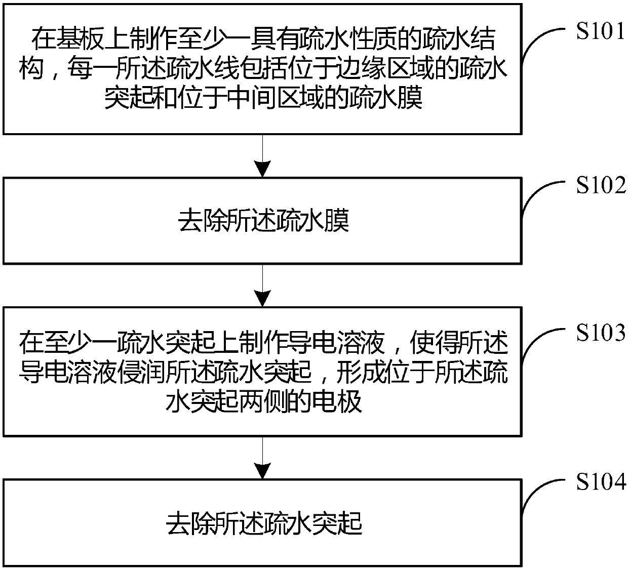
[0105] Next, fabricate the source electrode 250a and the drain electrode 250b on the gate insulating layer 230. The specific fabricating method of the source electrode 250a and the drain electrode 250b adopts the above-mentioned electrode fabricating method provided in the specific embodiment of the present invention, and specifically includes:

[0106] Firstly, a perfluororesin with hydrophobic properties is printed on the grid insulating layer 230 by inkjet printing, and the printed perfluororesin spontaneously form...

Embodiment 3

[0109] The fabrication of short-channel inorganic semiconductor thin film transistors with a top-gate and top-contact structure will be described in detail below.

[0110] Such as Figure 11 As shown, firstly, the inorganic semiconductor active layer 240 is fabricated on the substrate 100. The specific fabrication method of the inorganic semiconductor active layer 240 is the same as the fabrication method of Embodiment 1, and will not be repeated here.

[0111] Next, the source electrode 250a and the drain electrode 250b are manufactured on the inorganic semiconductor active layer 240. The specific manufacturing method of the source electrode 250a and the drain electrode 250b is the same as that of Embodiment 1, and will not be repeated here. The formed source electrode 250a The channel length d8 between the channel and the drain 250b does not exceed 5 μm.

[0112] Next, a gate insulating layer 230 and a gate 220 are fabricated sequentially on the source 250a and the drain 25...


PUM


Abstract

The invention discloses a manufacture method of an electrode, a TFT and a manufacture method thereof, an array substrate and a display panel, and aims at reducing the production cost and realizing large-area production. The manufacture method of the electrode comprises that at least one hydrophobic structure with a hydrophobic property is manufactured on a substrate, and each hydrophobic structurecomprises a hydrophobic projection positioned in the edge area and a hydrophobic film positioned in the middle area; the a hydrophobic film is removed; a conductive solution is made on the at least hydrophobic projection so that the hydrophobic projection is infiltrated with the conductive solution to form electrodes positioned at the two sides of the hydrophobic projection; and the hydrophobic projection is removed.

Description

technical field [0001] The invention relates to the technical field of semiconductors, in particular to a method for manufacturing an electrode, a thin film transistor and a method for manufacturing the same, an array substrate, and a display device. Background technique [0002] Oxide thin film transistors, as basic components for realizing electrical signal processing, control and transmission functions, are used in emerging fields such as flat panel display, flexible electronics and smart electronics. However, compared with traditional silicon-based microelectronic devices, oxide thin film transistors still have a large gap in terms of performance, stability, working speed and integration. [0003] At present, improving the working speed of oxide thin film transistors is generally achieved by increasing the mobility of oxide semiconductor materials, reducing channel length, and reducing parasitic capacitance. In the prior art, the working speed of the oxide thin film tra...

Claims


Application Information

Patent Timeline
Patent Type & Authority Applications(China)
IPC IPC(8): H01L21/28H01L29/786H01L29/06
CPCH01L21/28H01L29/06H01L29/786H01L29/41733H01L29/7869H01L27/124H01L27/1292H01L21/02109H01L21/02107H01L21/02112H01L21/0212H01L21/0273H01L21/0272H01L21/027H01L21/02118H01L21/02642H01L27/1262H01L29/42384H01L29/66742
Inventor 闫梁臣徐晓光兰林锋王磊彭俊彪
Owner BOE TECH GRP CO LTD
Why Eureka
Try Eureka