Gap detection device based on super-resolution lithography

A detection device and super-resolution technology, applied in measuring devices, optical devices, instruments, etc., can solve problems such as mask damage, and achieve the effect of ensuring the quality of photolithographic patterns

Active Publication Date: 2018-05-15
INST OF OPTICS & ELECTRONICS - CHINESE ACAD OF SCI
View PDF7 Cites 3 Cited by
  • Summary
  • Abstract
  • Description
  • Claims
  • Application Information

AI Technical Summary

Problems solved by technology

Obviously, this will cause mask damage

Method used


Image

  • Gap detection device based on super-resolution lithography
  • Gap detection device based on super-resolution lithography

Examples


Embodiment Construction

[0014] The present invention will be described in further detail below in conjunction with the accompanying drawings.

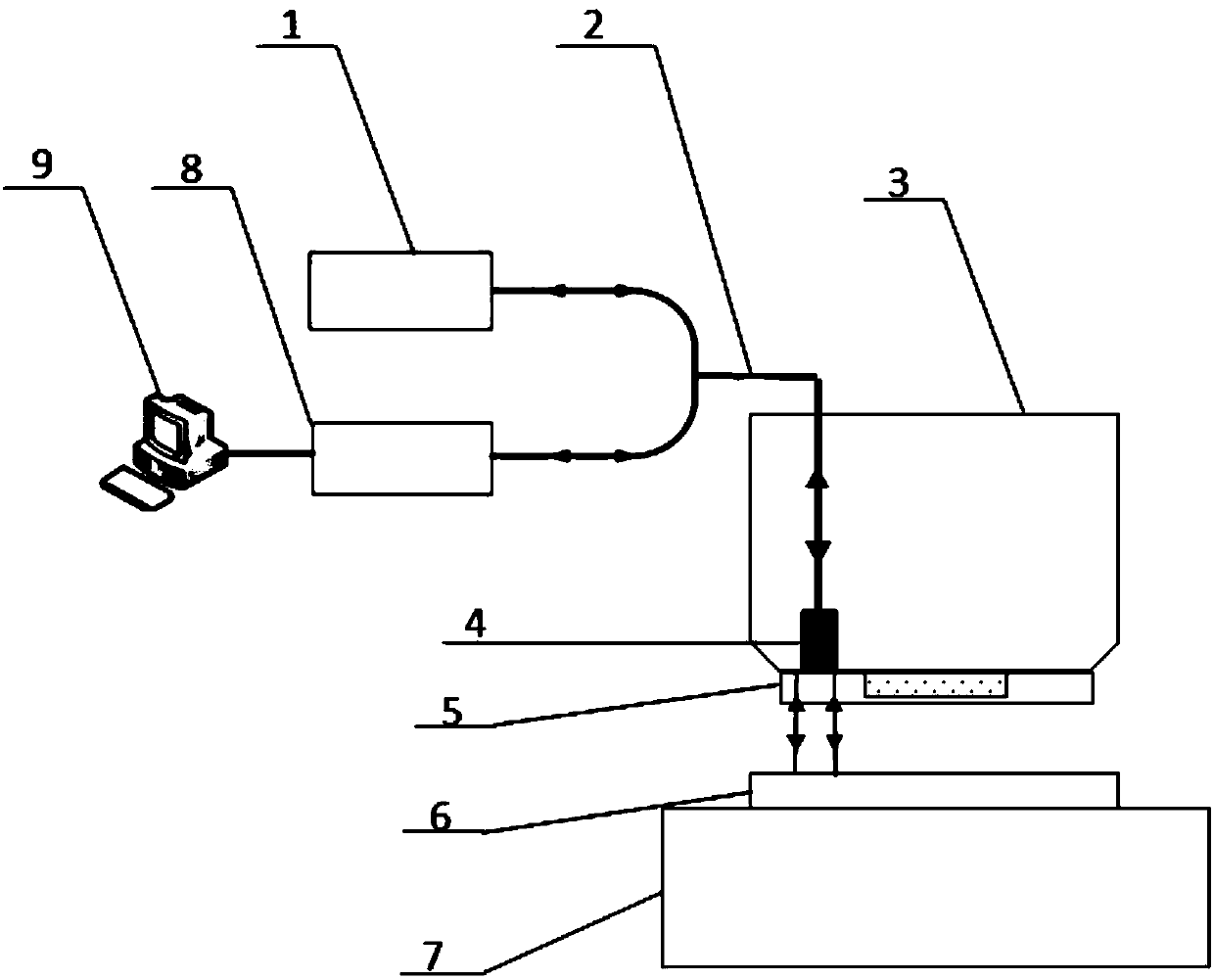
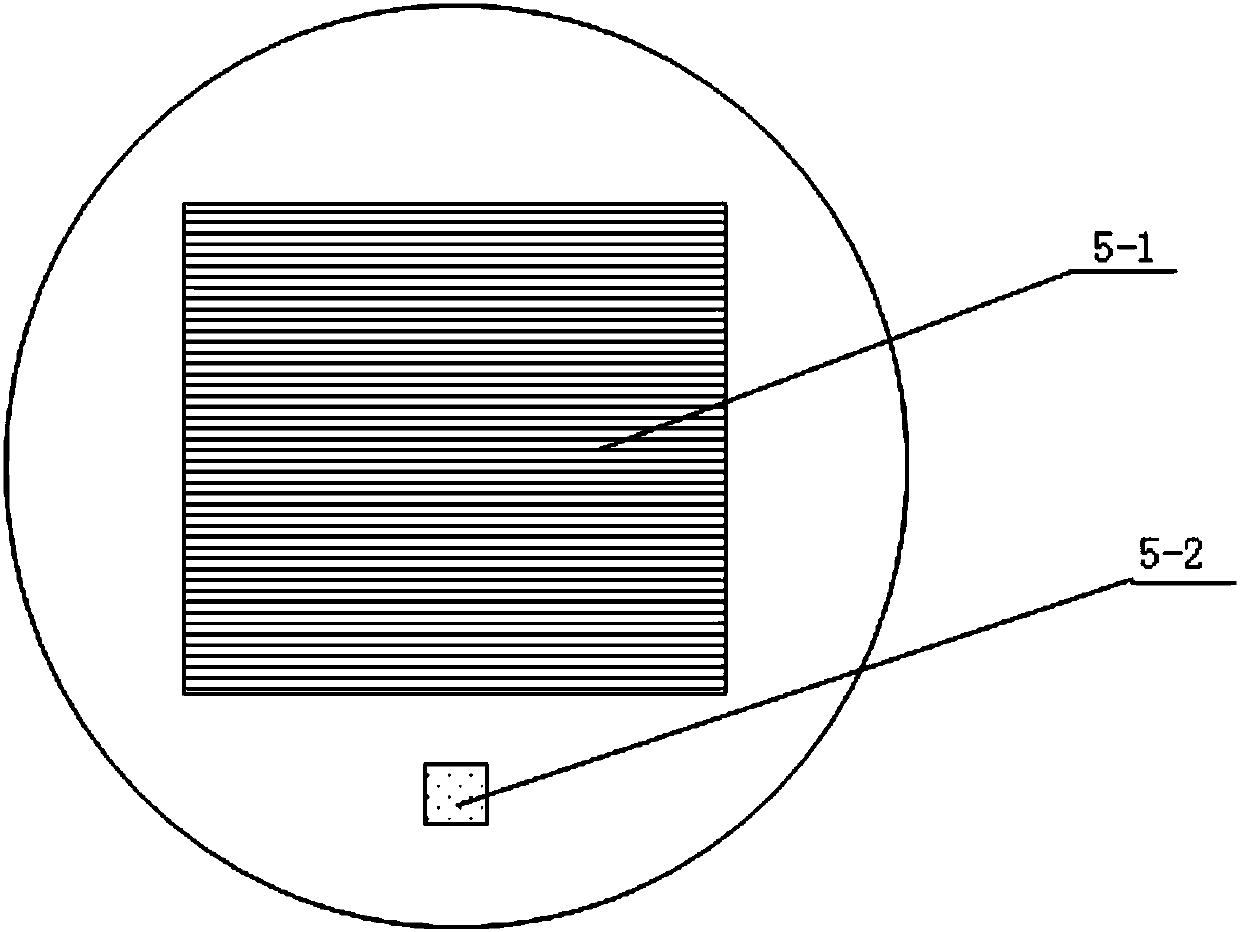
[0015] figure 1 It is a schematic diagram of a gap detection device for super-resolution lithography, which includes a white light source 1, a Y-shaped optical fiber 2, an objective lens frame 3, an optical fiber collimator mirror 4, a mask 5, a substrate 6, a nanometer workpiece table 7, a spectrometer 8 and PC9. Wherein the optical fiber collimator 4 and the mask 5 are clamped by the objective lens frame 3; the non-pattern area of ​​the mask 5 has a semi-transparent window, and the semi-transparent window is plated with a chromium layer, and the substrate 6 is plated with a silver layer. The light output from the white light source 1 is introduced into the optical fiber collimator 4 by the Y-shaped optical fiber 2, and the incident light is split in the semi-transparent and semi-reflective window under the mask 5, and a bunch of light is reflected back to...


PUM


Abstract

The invention provides a gap detection device based on super-resolution lithography. The light emitted by a light source is introduced into an optical fiber collimating mirror through a Y-shaped optical fiber, and is divided at a semi-transparent and semi-reflective window of a mask. One beam of light is reflected back into the optical fiber collimating mirror, and the other beam of light is transmitted by the semi-transparent and semi-reflective window of the mask, reflected by the surface of a substrate and received by the optical fiber collimating mirror through the semi-transparent and semi-reflective window of the mask. At the moment, a phase difference is generated due to the different optical paths of the two beams of light. The phase difference is detected through a spectrometer, and the phase difference corresponding to different wavelength is analyzed in a principal computer. Thus, the measurement of the absolute gap between the mask and the substrate is realized. The absolute value of the optical path difference between the substrate and the mask can be obtained, and further, the phase difference caused by the optical path difference between the substrate and the mask can be obtained, and the absolute gap between the mask and the substrate can be obtained. The gap is eliminated by controlling a nano work piece table, and gap exposure is realized. Therefore, a super-resolution lithography device is effectively protected, and the quality of lithography graphics is ensured.

Description

technical field [0001] The invention is a gap detection device based on super-resolution photolithography, and belongs to the technical field of nano-device manufacturing in ultra-large-scale integrated circuit manufacturing and optical micro-processing technology. Background technique [0002] The metalens imaging technology based on the surface plasmon effect is a new type of super-resolution optical imaging method that has attracted attention in recent years. Physically, this lithography technology belongs to near-field lithography, and its working distance is extremely short. Therefore, blowing, pressurization and vacuum suction are usually required to ensure the working distance during exposure. Obviously, this would cause mask damage. As we all know, masks are generally expensive, precision-processed pattern structures. In order to maintain a certain service life, the gap between the mask and the photolithographic substrate (working distance) should be extended while ...

Claims


Application Information

Patent Timeline
Patent Type & Authority Applications(China)
IPC IPC(8): G01B11/14
CPCG01B11/14
Inventor 冯金花唐燕何渝
Owner INST OF OPTICS & ELECTRONICS - CHINESE ACAD OF SCI
Why Eureka
Try Eureka