Automatic chip simulation and verification system

A chip system, simulation and verification technology, applied in special data processing applications, instruments, electrical digital data processing, etc., can solve the problems of time-consuming, labor-intensive, time-consuming and labor-intensive, and low degree of automation, and achieve high efficiency.

Inactive Publication Date: 2018-05-15
SUZHOU SAIYUAN MICROELECTRONICS
View PDF5 Cites 5 Cited by
  • Summary
  • Abstract
  • Description
  • Claims
  • Application Information

AI Technical Summary

Problems solved by technology

However, the traditional chip simulation verification takes a long time, the degree of automation is low, and it is time-consuming and laborious, which leads to a longer development cycle of the entire chip.
[0004] The traditional verification test mode is open-loop, requiring special personnel to manage and control input test vectors and observe simulation waveforms, which is time-consuming and labor-intensive
[0005] However, some automatic simulation platforms, such as PLI automatic simulation platform, also have various problems. 1) The PLI standard is complicated to use; 2) PLI must define system tasks or functions, and associate the calltf C function with the system task / function name; 3) The communication protocol interaction between the C model and the circuit is complex
This results in a high barrier to entry for using these automated emulation platforms

Method used


Image

  • Automatic chip simulation and verification system
  • Automatic chip simulation and verification system
  • Automatic chip simulation and verification system

Examples


Embodiment Construction

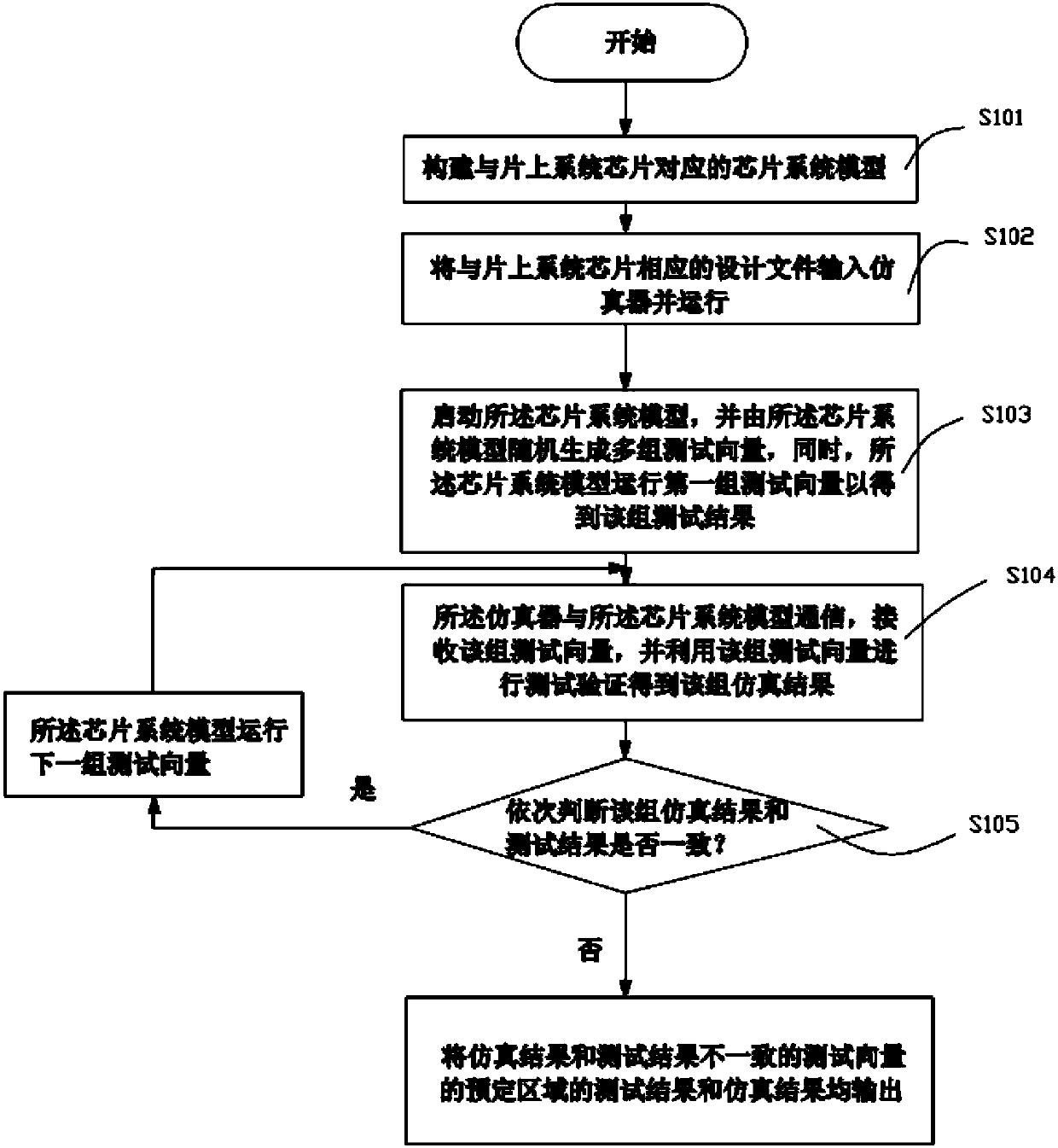
[0030] The following will clearly and completely describe the technical solutions in the embodiments of the present invention with reference to the accompanying drawings in the embodiments of the present invention. Obviously, the described embodiments are only some of the embodiments of the present invention, not all of them. Based on the embodiments of the present invention, all other embodiments obtained by persons of ordinary skill in the art without making creative efforts belong to the protection scope of the present invention.

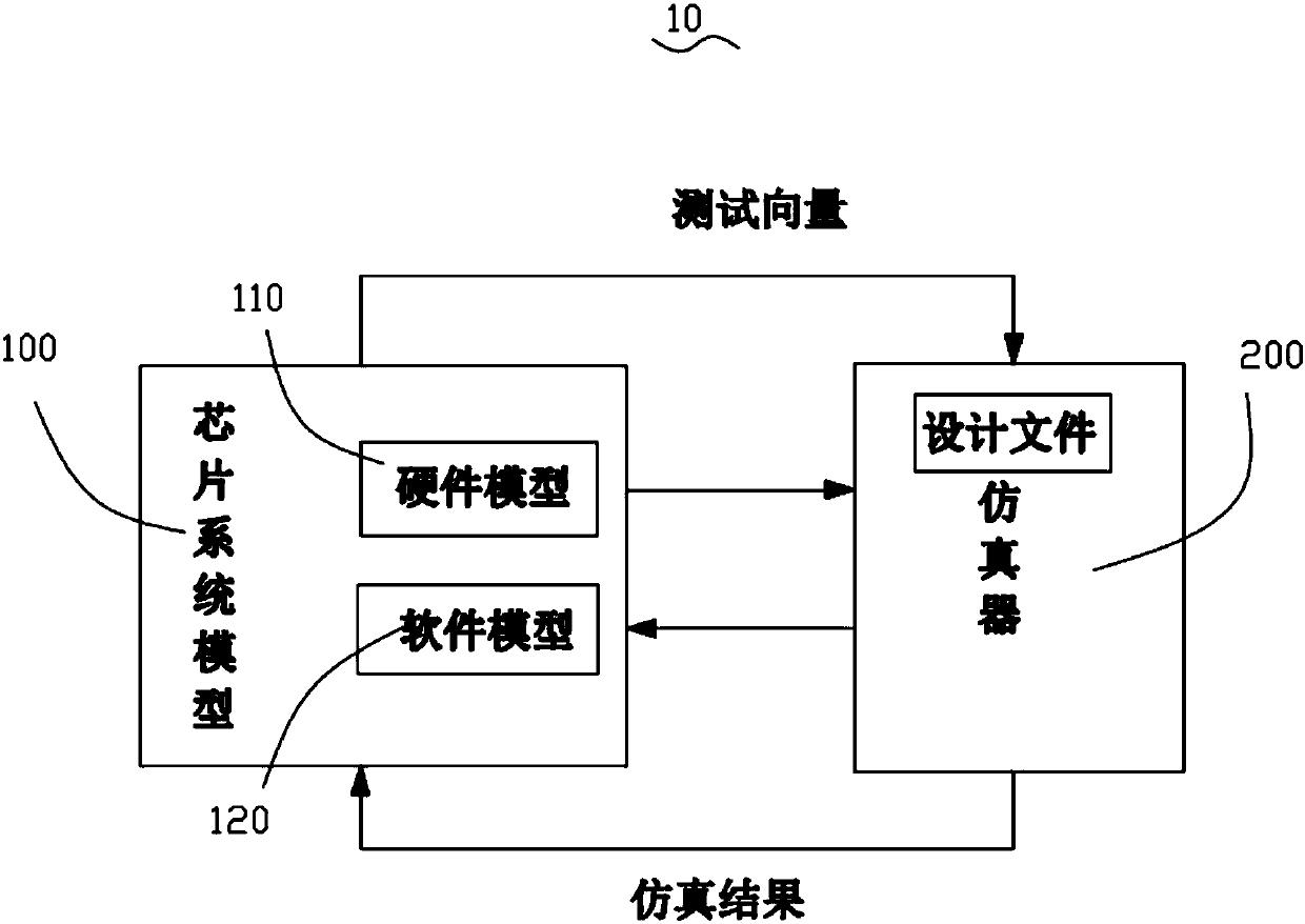
[0031] Schematic diagram of the SoC development process. The system-on-chip needs to go through the following main stages from the initial requirements to the final product: functional design, design description and behavior-level verification, logic synthesis, gate-level verification, layout and wiring, etc. The purpose of verification (verification) is to confirm that the functional correctness and performance (speed and power consumption, etc....


PUM


Abstract

The invention discloses an automatic chip simulation and verification system. The system comprises a chip system model, wherein the chip system model corresponds to a system-on-chip chip; a hardware model and a software model corresponding to the system-on-chip chip is established in the chip system model; the chip system model is used for randomly generating a plurality of groups of test vectorsand operating a test program; the test program is divided into a plurality of stages according to design and staged test results of the test are stored to units areas of a predetermined area; a simulator communicates with the chip system model; a simulation program of the simulator is divided into a plurality of simulation stages; staged simulation results of the simulation program are stored intounit areas of the predetermined area; and the chip system model is furthermore used for comparing the test results with the simulation results. According to the automatic chip simulation and verification system and method, automatic realization of the whole simulation and verification process is realized, so that the efficiency is relatively high; and the operation of constructing the chip systemmodel by utilizing abstract-level languages which comprise a hardware description language is relatively simple.

Description

technical field [0001] The invention relates to the technical field of detection of chip products, in particular to a chip automatic simulation verification system. Background technique [0002] System On Chip (System On Chip, SOC) refers to the integration of all functional systems required for microelectronic application products on a single chip, which is based on Very Deep Submicron (VDSM) technology and intellectual property (Intellectual Property, IP ) nuclear multiplexing technology as the support. SOC technology is the current development trend of Very Large Scale Integrate (VLSI), and it is also the main technology and method to solve Time to Market (TTM) in the development of electronic products. [0003] With the rapid development of deep submicron technology, the integration scale of chips is getting larger and larger, and the verification of chip functions has become more and more important and complex and time-consuming, and the design methods of chips have al...

Claims


Application Information

Patent Timeline
IPC IPC(8): G06F17/50
CPCG06F30/30G06F30/398
Inventor 樊超
Owner SUZHOU SAIYUAN MICROELECTRONICS
Why Eureka
Try Eureka