Method of manufacturing semiconductor device

A manufacturing method and semiconductor technology, applied in semiconductor/solid-state device manufacturing, semiconductor devices, transistors, etc., can solve the problem of short carrier life

Active Publication Date: 2018-05-25
DENSO CORP
View PDF5 Cites 6 Cited by
  • Summary
  • Abstract
  • Description
  • Claims
  • Application Information

AI Technical Summary

Problems solved by technology

In crystal defect regions, the carrier lifetime is short

Method used


Image

  • Method of manufacturing semiconductor device
  • Method of manufacturing semiconductor device
  • Method of manufacturing semiconductor device

Examples


Embodiment Construction

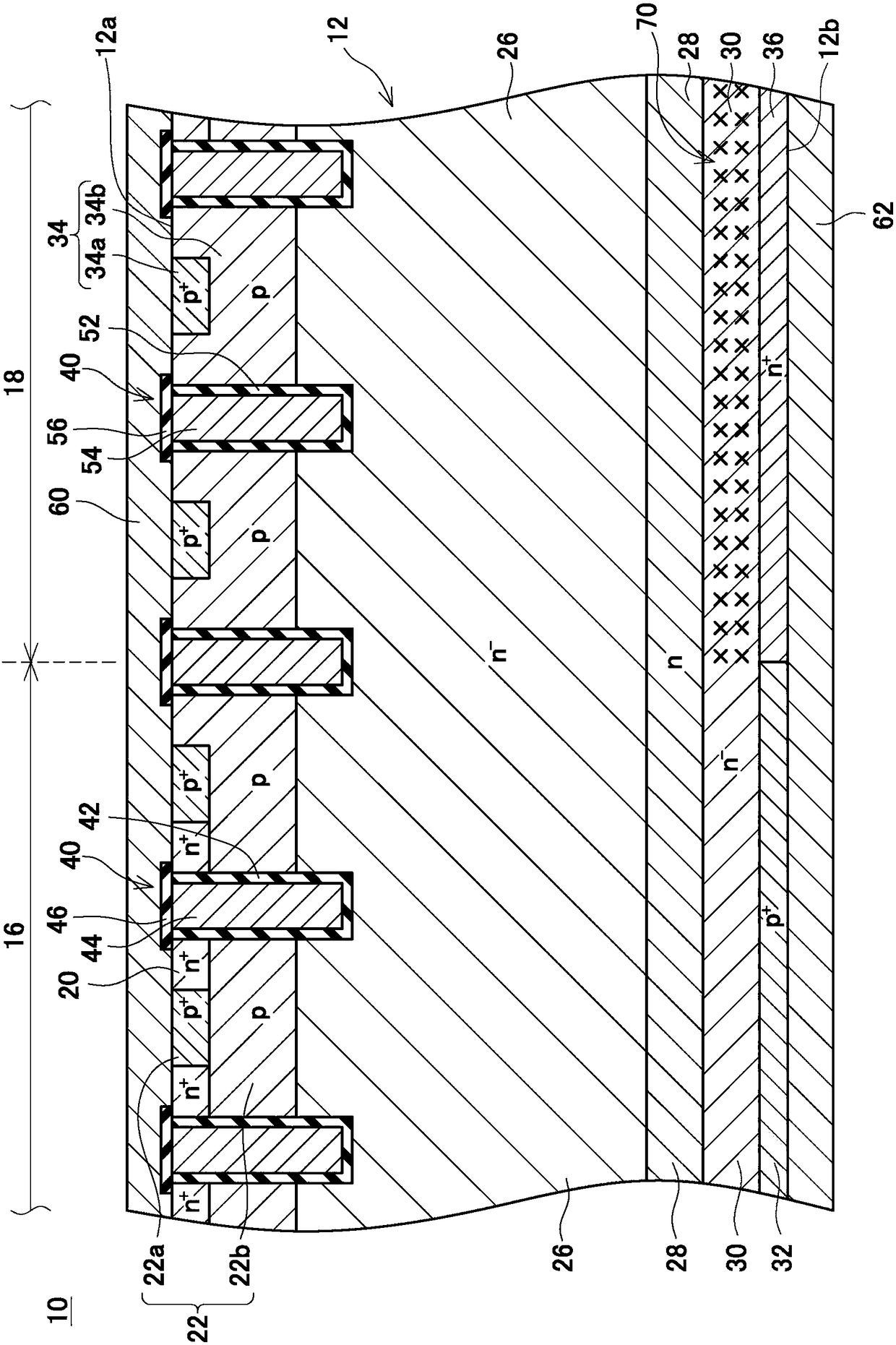
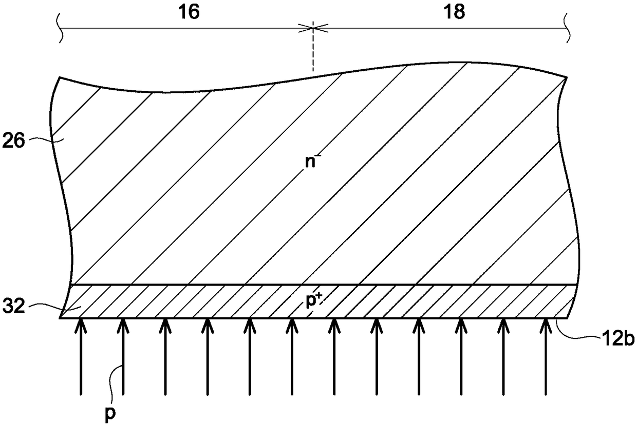
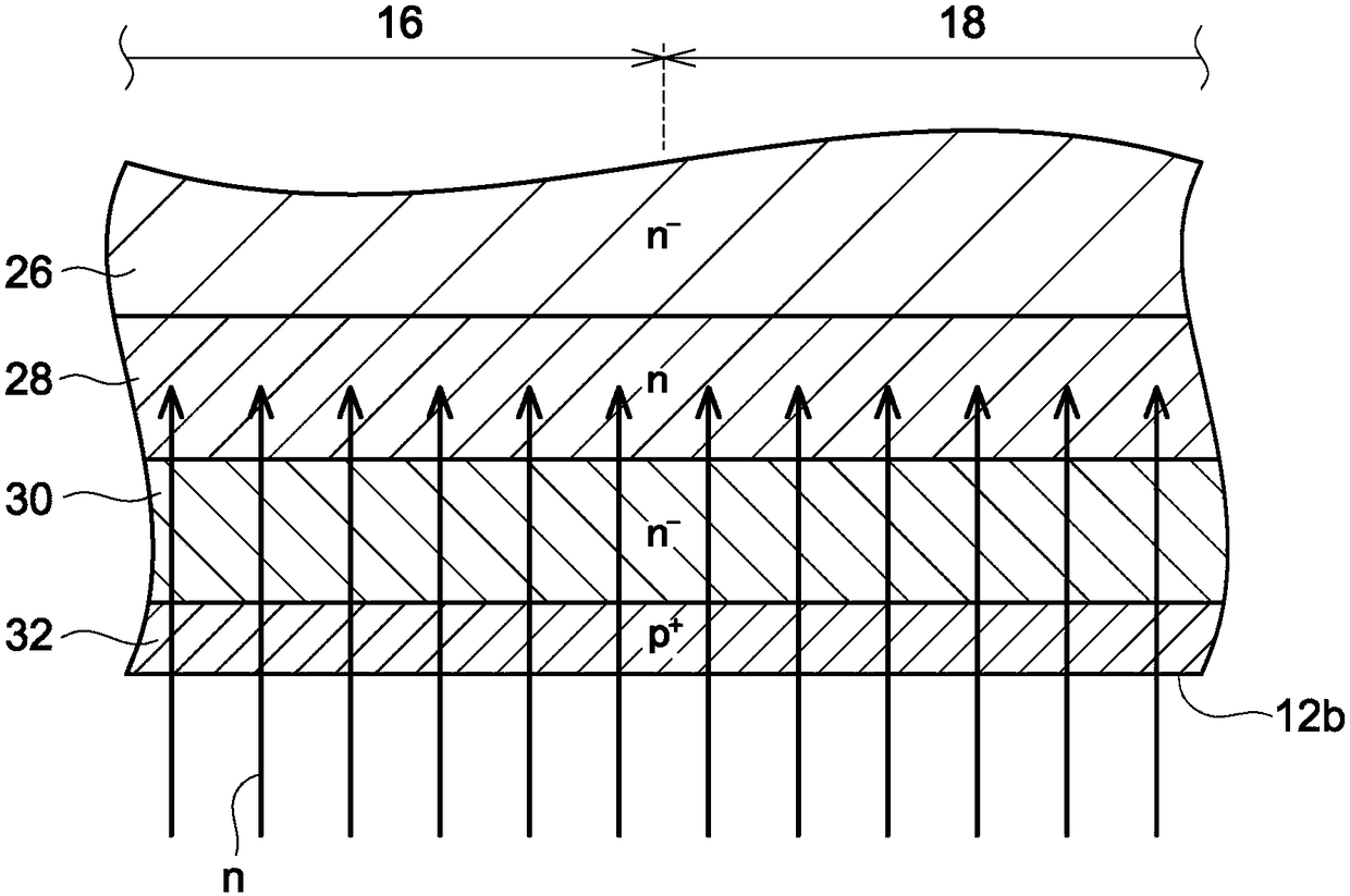
[0020] figure 1 A semiconductor device 10 manufactured by the method of this embodiment is shown. The semiconductor device 10 is composed of a semiconductor substrate 12 , electrodes, insulators, and the like provided on the upper surface 12 a and the lower surface 12 b of the semiconductor substrate 12 . The semiconductor substrate 12 is made of silicon. The semiconductor substrate 12 includes an IGBT region 16 and a diode region 18 . The IGBT region 16 is adjacent to the diode region 18 when the semiconductor substrate 12 is viewed planarly along the thickness direction of the semiconductor substrate 12 . IGBTs are provided in the IGBT region 16 , and diodes are provided in the diode region 18 . That is, the semiconductor device 10 is a so-called RC-IGBT.

[0021] A plurality of grooves 40 are provided on the upper surface 12 a of the semiconductor substrate 12 . Each groove 40 is along with figure 1 The directions perpendicular to the paper surface extend parallel to ...


PUM


Abstract

The present invention provides a method of manufacturing a semiconductor device that allows suppressing the relative positional misalignment between a cathode region and a crystal defect region. The method of manufacturing a semiconductor device having a diode includes: implanting charged particles into a first range and a second range in a semiconductor substrate from at least one of a first surface of the semiconductor substrate and a second surface of the semiconductor substrate located on an opposite side of the first surface so as to increase crystal defect densities in the first range and the second range; implanting n-type impurities into the first range from the first surface so as to make a region amorphous, the region being in the first range and disposed at the first surface; irradiating the first surface with first laser after the implantation of the charged particles and the implantation of the n-type impurities so as to heat the first range and the second range; and crystallizing the region which has been made amorphous in or after the irradiation of the first laser.

Description

technical field [0001] The technology disclosed in this specification relates to a method of manufacturing a semiconductor device. Background technique [0002] Patent Document 1 discloses a semiconductor device (so-called RC-IGBT (Reverse Conducting-Insulated Gate Bipolar Transistor: Reverse Conducting Insulated Gate Bipolar Transistor)) including an IGBT and a diode. A region (hereinafter referred to as a crystal defect region) in which the density of crystal defects is increased by implantation of charged particles is provided inside the diode. Crystal defect regions are not provided outside the diode (for example, inside the IGBT). In crystal defect regions, the carrier lifetime is short. By providing a crystal defect region inside the diode, the reverse recovery characteristic of the diode can be improved. [0003] prior art literature [0004] patent documents [0005] Patent Document 1: Japanese Patent Laid-Open No. 2008-192737 Contents of the invention [000...

Claims


Application Information

Patent Timeline
Patent Type & Authority Applications(China)
IPC IPC(8): H01L21/331H01L21/268H01L21/322H01L29/739
CPCH01L21/268H01L21/322H01L29/66348H01L29/7397H01L27/0727H01L29/36H01L29/8613H01L29/407H01L29/0834H01L29/32H01L21/26513H01L27/0716H01L29/08H01L29/8611H01L21/8249
Inventor 细川博司岩崎真也西胁刚今井敦志大木周平
Owner DENSO CORP
Why Eureka
Try Eureka