Storage array control method and device based on multiple channels of NandFlash memory

A storage array and control device technology, applied in the storage field, to reduce the bus time occupied by a single Flash, improve the limitation of write operation characteristics, and improve the overall read and write performance

Pending Publication Date: 2018-06-05
HONGQIN (BEIJING) TECHNOLOGY CO LTD
View PDF0 Cites 23 Cited by
  • Summary
  • Abstract
  • Description
  • Claims
  • Application Information

AI Technical Summary

Problems solved by technology

[0005] The present invention provides a storage array control method and device based on multi-channel N

Method used


Image

  • Storage array control method and device based on multiple channels of NandFlash memory
  • Storage array control method and device based on multiple channels of NandFlash memory
  • Storage array control method and device based on multiple channels of NandFlash memory

Examples


Embodiment Construction

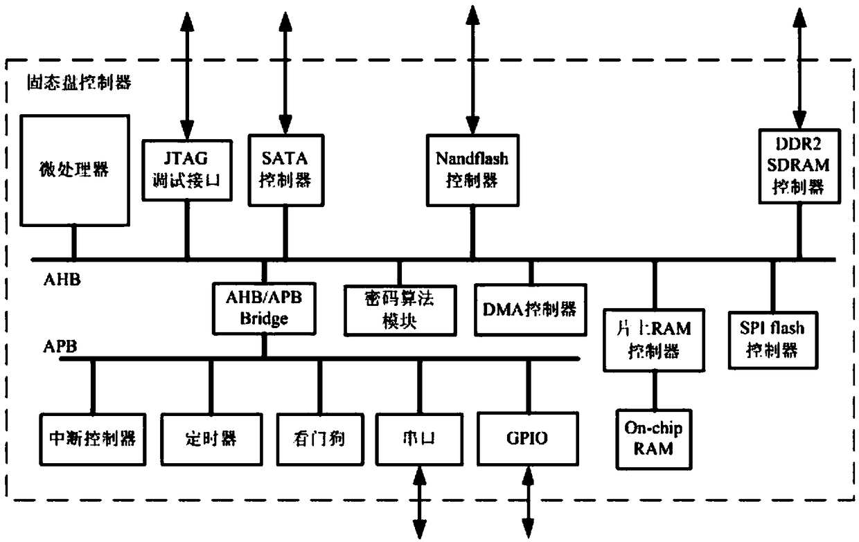
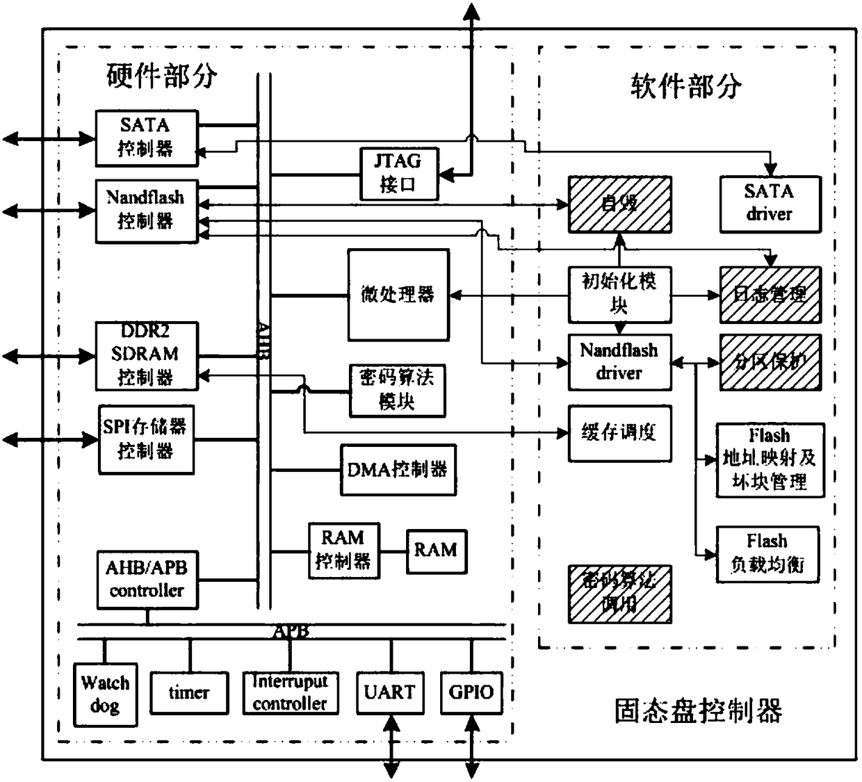
[0053] The storage array control method and device based on the multi-channel NandFlash memory provided by the present invention firstly describes the solid-state disk controller.

[0054] 1. Working principle of SSD controller

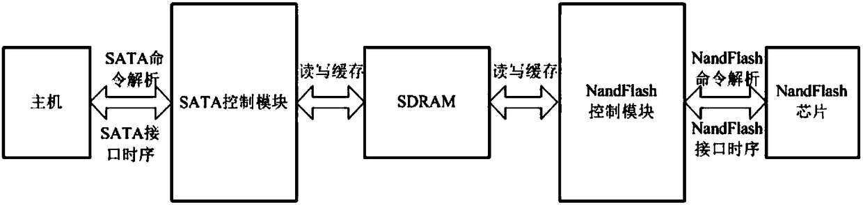
[0055] The solid-state disk controller implements the interface function from the host SATA (Serial Advanced Technology Attachment, Chinese is the serial ATA interface specification) end to the NandFlash memory chip end, it analyzes the SATA command sent by the host, converts it into the instruction of the NandFlash chip, and writes the data into or read out of NandFlash to complete the data transfer between the SSD and the host, such as figure 1 shown.

[0056] The host's access to the SSD is generally divided into two types: data transfer commands and non-data transfer commands. For commands that require data transmission, when the SSD controller processes them, it first analyzes the data transmission direction (read / write), transmission length, d...


PUM


Abstract

The invention provides a storage array control method and device based on multiple channels of a NandFlash memory. The device includes an embedded-type microprocessor, and the embedded-type microprocessor is connected with each external module through an in-chip high-speed intercommunication bus; the external modules include the SATA controller, the Nandflash controller, the DDR2 SDRAM controller,the JTAG debugging interface, the AHB/APB bridge, the code algorithm module, the DMA controller, the on-chip RAM controller and the SPI flash controller. The AHB/APB bridge connects the in-chip high-speed intercommunication bus with an in-chip low-power-consumption intercommunication bus, the in-chip low-power-consumption intercommunication bus is connected with an interrupt controller, a timer,a watchdog, a serial port and a GPIO, and therefore a complete on-chip system is constructed. The control method is designed on the basis of an assembly line framework and a fully-connected parallel framework, parallel running of the channels and an assembly line operation are achieved, the access bandwidth of a Flash interface is fully utilized, and the system performance is further improved.

Description

technical field [0001] The invention relates to the field of storage technology, in particular to a storage array control method and device based on multi-channel NandFlash memory. Background technique [0002] Computer bus technology and semiconductor storage technology have promoted the rapid development and maturity of high-speed data storage. In recent years, in terms of transmission rate, the rapid development of electronic technology has promoted the development of high-speed serial bus for the Internet of Things, cloud computing and big data testing, and the traditional parallel transmission technology has become a bottleneck for improving data transmission rate. Commonly used serial buses include USB interface technology, Gigabit / 10 Gigabit Ethernet communication technology, optical fiber interface technology, and PCI-E bus technology. The transmission rate of the latest USB3.0 interface can reach 5Gb / s, and the transmission rate of Ethernet and optical fiber interf...

Claims


Application Information

Patent Timeline
IPC IPC(8): G06F13/16
CPCG06F13/1673Y02D10/00
Inventor 张涛周洋武恒基吕景成
Owner HONGQIN (BEIJING) TECHNOLOGY CO LTD
Why Eureka
Try Eureka