Vertical-structure double-color LED based on GaN material, and preparation method for vertical-structure double-color LED
A vertical structure, two-color technology, applied in electrical components, circuits, semiconductor devices, etc., can solve the problems of difficult packaging and poor reliability, and achieve the effect of reducing LED cost, improving integration, and flexible color temperature adjustment.
- Summary
- Abstract
- Description
- Claims
- Application Information
AI Technical Summary
Problems solved by technology
Method used
Image
Examples
Embodiment 1
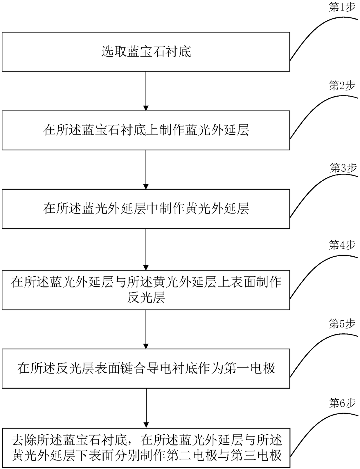
[0055] See figure 1 , figure 1 A flow chart of a method for preparing a GaN material-based vertical-structure two-color LED provided in an embodiment of the present invention, the method includes:
[0056] (a) select a sapphire substrate;
[0057] (b) making a blue epitaxial layer on the sapphire substrate;
[0058] (c) making a yellow epitaxial layer in the blue epitaxial layer;
[0059] (d) making a reflective layer on the upper surface of the blue epitaxial layer and the yellow epitaxial layer;
[0060] (e) bonding a conductive substrate on the surface of the reflective layer as the first electrode;
[0061] (f) removing the sapphire substrate, and forming a second electrode and a third electrode on the lower surfaces of the blue epitaxial layer and the yellow epitaxial layer respectively.
[0062] Wherein, the crystal plane of the sapphire substrate is (0001).
[0063] For step (b), it may include:
[0064] (b1) growing a first GaN buffer layer with a thickness of 3...
Embodiment 2
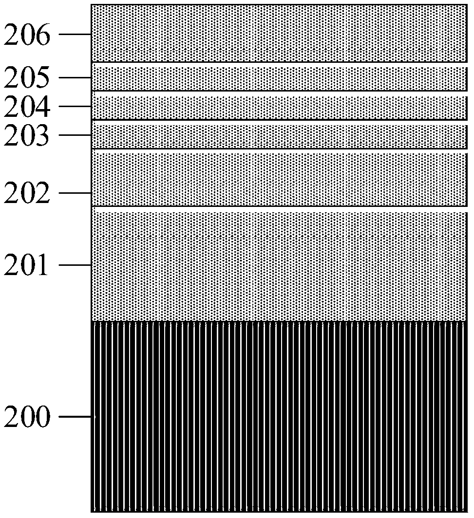
[0095] Please refer to Figure 2a ~ Figure 2g , Figure 2a ~ Figure 2g It is a schematic diagram of a method for preparing a GaN material-based vertical structure two-color LED according to an embodiment of the present invention. Specifically, the preparation method comprises the following steps:
[0096] The 1st step, select the sapphire substrate 200 that thickness is 4000nm, as Figure 2a shown.
[0097] Step 2. At a temperature of 500°C, grow a first GaN buffer layer 201 with a thickness of 4000nm on the upper surface of the sapphire substrate 200; at a temperature of 1000°C, grow a thickness of A first GaN stable layer 202 of 1000 nm; at a temperature of 1000° C., grow on the surface of the first GaN stable layer 202 with a thickness of 400 nm and a doping concentration of 1×10 19 cm -3 The first n-type GaN layer 203; the first InGaN quantum well / first GaN barrier multiple structure is grown on the surface of the first n-type GaN layer 203 as the first active layer 2...
Embodiment 3
[0105] Please refer to image 3 , image 3 It is a structural schematic diagram of a GaN material-based vertical two-color LED according to an embodiment of the present invention. This embodiment focuses on the structure of the LED of the present invention under the process flow described in the above embodiments as follows. Specifically, the LED 500 includes a conductive substrate 501 , a reflective layer 502 , a blue epitaxial layer 503 , a yellow epitaxial layer 504 , an isolation layer 505 and an electrode 506 . The electrode 506 is preferably a conductive substrate, and of course other conductive materials can be selected as the electrode 506, such as Au, Al, etc., without any limitation here.
[0106] In this embodiment, by integrating the blue light and the yellow light on the same chip, the amount of fluorescent powder is reduced, and at the same time, the conductive substrate is used as the electrode, which is beneficial to the heat dissipation of the LED chip.
PUM
| Property | Measurement | Unit |
|---|---|---|
| Thickness | aaaaa | aaaaa |
| Thickness | aaaaa | aaaaa |
| Thickness | aaaaa | aaaaa |
Abstract
Description
Claims
Application Information


