Preparation method and application of 3D polarizing film and 3D display device and display system

A display device and polarizing film technology, applied in optics, polarizing elements, optical elements, etc., can solve problems such as limited use effect, polarizer thickness, and large crosstalk interval, so as to improve production and bonding efficiency and compensate for surface flatness Poor degree, the effect of improving production efficiency

Active Publication Date: 2020-04-24
NINGBO VISION DISPLAY TECH
View PDF7 Cites 2 Cited by
  • Summary
  • Abstract
  • Description
  • Claims
  • Application Information

AI Technical Summary

Problems solved by technology

[0007] Although this method has improved efficiency compared with the method of laminating strips one by one, it is difficult to implement for small-pitch LEDs due to the thicker polarizers, higher hardness, and depressions on the edges after punching. Can only be used for display devices above P2.5
[0008] At the same time, in the above two existing methods, both left and right rotating polarizers are spliced, and the splicing error is twice the punching error, which is prone to cumulative errors and the crosstalk interval is large.
At the same time, the surface flatness of the laminated product is poor, and the reflectivity of the surface is high, the actual use effect is limited

Method used


Image

  • Preparation method and application of 3D polarizing film and 3D display device and display system
  • Preparation method and application of 3D polarizing film and 3D display device and display system
  • Preparation method and application of 3D polarizing film and 3D display device and display system

Examples


preparation example Construction

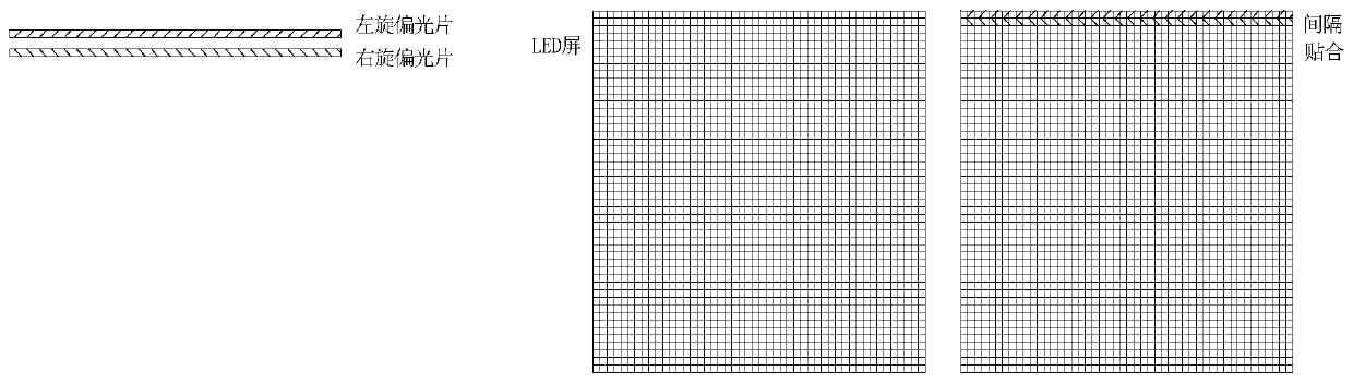
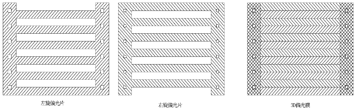
[0063] It can be known from the above steps of the preparation method that the method of the present invention adopts the method of laminating the retardation film and the polarizing film to form a 3D polarizing film. Only one die-cutting is carried out, and the complex operations brought about by the traditional patchwork lamination are avoided through sheet lamination, which greatly improves the production and lamination efficiency;

[0064] At the same time, since there is no need for splicing between different polarizing films, at least half of the splicing error can be reduced;

[0065] Further, the follow-up filling process of the present invention also effectively makes up for the defects of large surface flatness of traditional products, and can more efficiently produce high-quality, small-pitch 3D polarizing films, especially for 3D polarizing films for LED and OLED displays. Polarizing film.

[0066] At the same time, the present invention also provides a 3D display...

Embodiment 1

[0071] Please refer to Figure 3-8 As shown in the process, the preparation method of the 3D polarizing film provided in this embodiment is as follows:

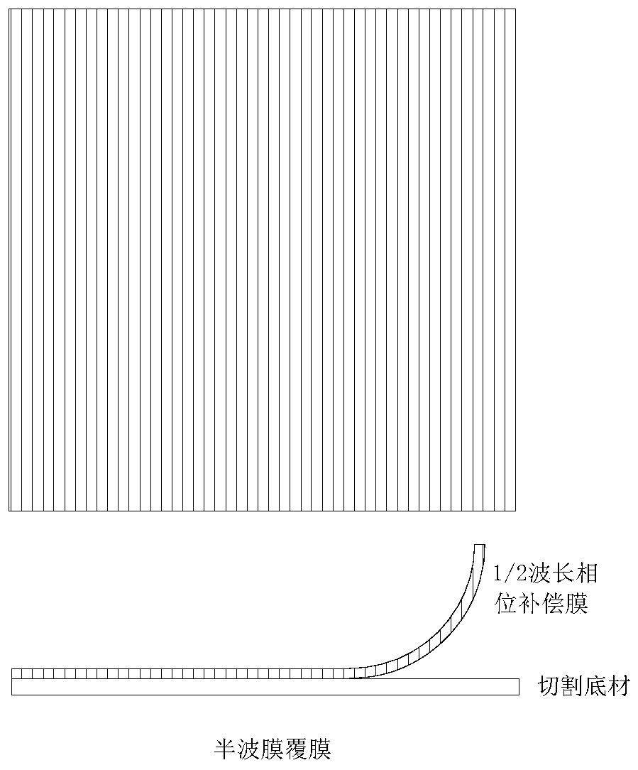
[0072] (a) 1 / 2 wavelength retardation compensation film is attached with a cut base film;

[0073] (b) Die-cutting the 1 / 2 wavelength retardation compensation film with a cut base film to form a patterned structure with a thickness of 0.03 mm;

[0074] (c) peeling off the invalid regions in the resulting patterned structure;

[0075] (d) filling the surface of the stripped patterned structure with glue to form a planarization layer;

[0076] (e) punching the gained film to form a patterned retardation film;

[0077] (f) Bonding the retardation film and the left-handed polarizer to obtain the 3D polarizing film of Example 1, the thickness of which is 0.15 mm.

[0078] Further, the 3D polarizing film prepared in Example 1 is pasted on the surface of the LED display unit, so that the 3D display device of Example 1 can be obt...

Embodiment 2

[0080] Please refer to Figure 3-8 As shown in the process, the preparation method of the 3D polarizing film provided in this embodiment is as follows:

[0081] (a) 1 / 2 wavelength retardation compensation film is attached with a cut base film;

[0082] (b) Die-cutting the 1 / 2 wavelength retardation compensation film with a cut base film to form a patterned structure with a thickness of 0.02 mm;

[0083] (c) peeling off the invalid regions in the resulting patterned structure;

[0084] (d) filling the surface of the stripped patterned structure with glue to form a planarization layer;

[0085] (e) punching the gained film to form a patterned retardation film;

[0086] (f) Bonding the retardation film and the right-handed polarizer to obtain the 3D polarizing film of Example 2, the thickness of which is 0.20 mm.

[0087] Further, the 3D polarizing film prepared in Example 2 was pasted on the surface of the OLED liquid crystal unit, so as to obtain the 3D display device in Ex...


PUM

PropertyMeasurementUnit
thicknessaaaaaaaaaa
thicknessaaaaaaaaaa
thicknessaaaaaaaaaa

Abstract

The invention provides a 3D polarizing film, a manufacturing method and an application, a 3D display device including the 3D polarizing film and a display system. In the method, through sheet-shaped pasting, production and pasting efficiency is greatly increased; and through punching a phase delay film with a dozens of micrometer thickness, accurate manufacturing of the3D polarizing film of a small spacing is realized. In the invention, splicing of the films is not needed and a splicing seam error is reduced by half; simultaneously, through a filling and leveling-up technology, the defect thatproduct surface flatness is poor is overcome. The manufacturing method is suitable for manufacturing various 3D polarizing films and a further-polarized LED stereoscopic display device. Production efficiency is greatly increased and simultaneously production and manufacturing of the high-quality and small-spacing LED 3D polarizing film and the corresponding polarizing-type LED stereoscopic display device can be realized.

Description

technical field [0001] The invention relates to the technical field of stereoscopic display, in particular, to a 3D polarizing film, a preparation method and application thereof, and a 3D display device and a display system comprising the same. Background technique [0002] Polarized stereoscopic display is a 3D display method that uses the principle of "vibration direction" of light to realize the decomposition of the original image and stereoscopic imaging. It mainly uses left-handed and right-handed polarizing films on adjacent rows of the display device In this way, two images with different polarization directions are sent to the viewer. When the images pass through the polarized glasses, since each lens of the polarized glasses can only accept images with one polarization direction, the left and right eyes of the person can receive two sets of images. The screen is then synthesized into a three-dimensional image by the brain. [0003] At present, the polarizing film i...

Claims


Application Information

Patent Timeline
Patent Type & Authority Patents(China)
IPC IPC(8): G02B5/30G02B30/25
CPCG02B5/3083G02B30/25
Inventor 张勇王华波顾开宇张春光
Owner NINGBO VISION DISPLAY TECH
Why Eureka
Try Eureka