Electronic product production process

A production process and technology for electronic products, which is applied in the manufacture of circuits, electrical components, semiconductors/solid-state devices, etc., can solve the problems of high friction on the surface of the protective film, easy scratching of the protective film, and exposure of IC patterns. Good effect, good grinding effect, and the effect of reducing friction

Active Publication Date: 2020-03-24
广西格思克实业有限责任公司
View PDF7 Cites 0 Cited by
  • Summary
  • Abstract
  • Description
  • Claims
  • Application Information

AI Technical Summary

Problems solved by technology

[0005] However, in the existing wafer placement equipment, the following problems often occur: during the placement process, the protective film is often pasted on the front of the wafer by sliding friction. This method of placement makes the friction force on the surface of the protective film Larger, the protective film is easily scratched, resulting in the process of grinding the wafer with the front side down, the IC pattern on the wafer surface is easily exposed from the protective film and damaged, resulting in the failure of the wafer and improving the quality of the wafer. round defect rate

Method used


Image

  • Electronic product production process
  • Electronic product production process

Examples


Embodiment 1

[0030] The embodiment is basically as attached figure 1 Shown:

[0031] The electronic product production process includes the following steps:

[0032] 1) Wafer preparation: Clean the wafer surface with a cleaning solution, the cleaning solution includes ammonia water and hydrogen peroxide, and NH 3 :H 2 o 2 :H 2 The mass ratio of O is 1:1-2:150-200; then dry the wafer with cold air.

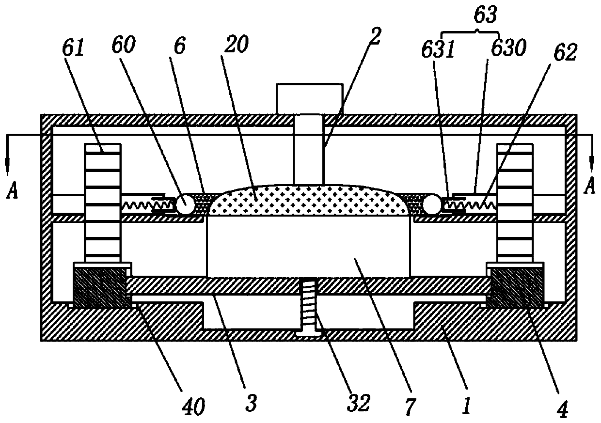
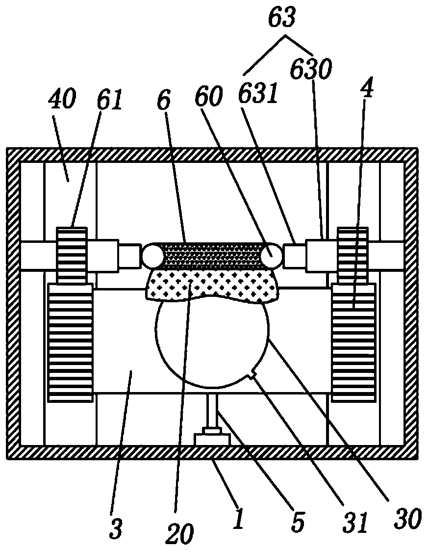
[0033] 2) Mounter preparation: The mounter includes a frame 1, a mount mechanism 2, a moving mechanism and a flattening mechanism. Wherein, the placement mechanism 2 may adopt a structure in the prior art, that is, a structure capable of pulling the protective film 20 to the surface of the wafer 7 and performing subsequent cutting. like figure 2 As shown, the moving mechanism includes a support plate 3, a sliding rack 4, and a mover for translation of the support plate 3. The mover in this embodiment is a moving pneumatic cylinder 5. Of course, a hydraulic cylinder can also be used to r...

Embodiment 2

[0045] The difference between the present invention and Example 1 is that the cleaning solution in step 1) includes ammonia and hydrogen peroxide, and the NH 3 :H 2 o 2 :H 2 The mass ratio of O is 1:2:200; in step 8), the wafer is ground to a thickness of 350um.


PUM


Abstract

The invention belongs to the technical field of electronic product production, and specifically relates to a production technology for an electronic product. The technology comprises the following steps: 1), wafer preparation: cleaning the surface of a wafer through cleaning fluid, and drying the wafer through cold air; 2), chip mounter preparation; 3), feeding: fixing the wafer on a support plateof a chip mounter at step 2); 4), positioning: starting a moving device at step 2), and enabling the support plate to translate below a flattened air bag; 5), chip mounting: pasting a protection filmon the upper surface of the wafer, continuing to translate the support plate at the same time, and enabling the flat air bag to flatten the protection film in a rolling state; 6), cutting: cutting the redundant protection film, and completing the chip mounting; 7), grinding: grinding the wafer till the thickness is 180-350 microns after chip mounting; 8), chip tearing: tearing off the protectionfilm at step 2). According to the scheme of the invention, the method can effectively prevent the bubbles generated between the protection film and the wafer in a chip mounting process, and reduces the reject ratio of the wafer.

Description

technical field [0001] The invention belongs to the technical field of electronic product production, and in particular relates to an electronic product production process. Background technique [0002] Electronic products refer to electronic products used in daily consumer life. It is a specific household appliance that contains electronic components and is usually used for entertainment, communication, and clerical purposes, such as telephones, audio equipment, televisions, DVD players, and even electronic clocks. Chips, also known as microcircuits, microchips, and integrated circuits, refer to silicon chips containing integrated circuits. They are small in size and are the most important part of electronic products, undertaking the functions of computing and storage. The complete process of chip production includes several links such as chip design, wafer production, packaging production, and cost testing; the raw material for its production is wafers. Wafer refers to t...

Claims


Application Information

Patent Timeline
Patent Type & Authority Patents(China)
IPC IPC(8): H01L21/02
CPCH01L21/02H01L21/02002H01L21/02052
Inventor 廖洪清
Owner 广西格思克实业有限责任公司
Why Eureka
Try Eureka