Composite conductive antireflective film for crystalline silicon heterojunction solar cell

A solar cell, composite conductive technology, applied in circuits, photovoltaic power generation, electrical components, etc., can solve problems such as high temperature and affecting material transmittance

Active Publication Date: 2018-06-19
INST OF ELECTRICAL ENG CHINESE ACAD OF SCI
View PDF6 Cites 0 Cited by
  • Summary
  • Abstract
  • Description
  • Claims
  • Application Information

AI Technical Summary

Problems solved by technology

At present, through conventional sputtering technology, the substrate is parallel to the surface of the target, and the optimized deposition parameters have been able to prepare randomly arranged ITO nanowhiskers, but the temperature used is relatively high, generally around 300 ° C, and Au is mostly used. and other metal catalysts, which will inevitably affect the transmittance of the material

Method used


Image

  • Composite conductive antireflective film for crystalline silicon heterojunction solar cell
  • Composite conductive antireflective film for crystalline silicon heterojunction solar cell
  • Composite conductive antireflective film for crystalline silicon heterojunction solar cell

Examples


Embodiment 1

[0034] A high-purity indium oxide ceramic target with a hafnium dioxide doping amount of 1.25wt.% was used, the substrate temperature was 200°C, and the hydrogen partial pressure was 5×10 -2 Pa.

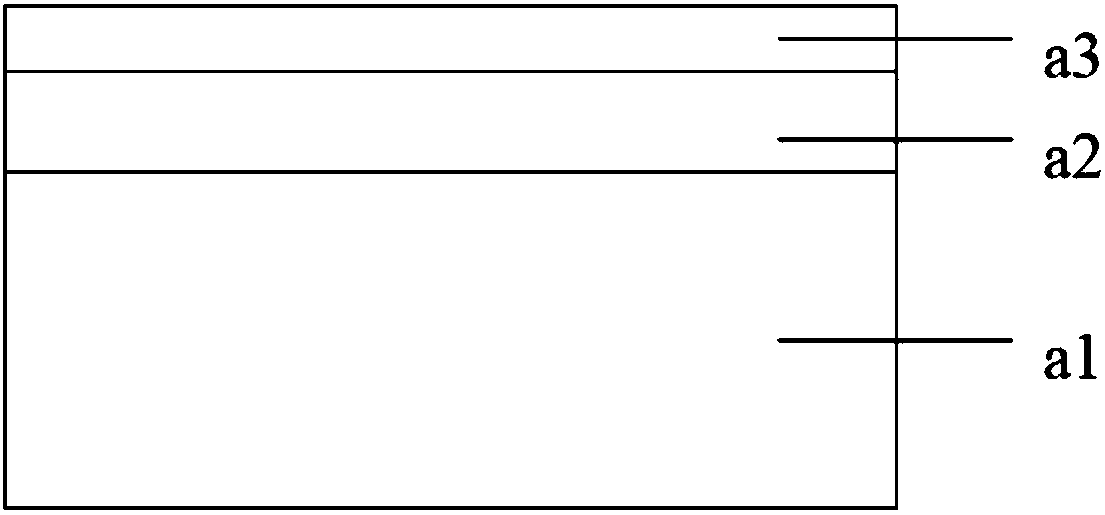
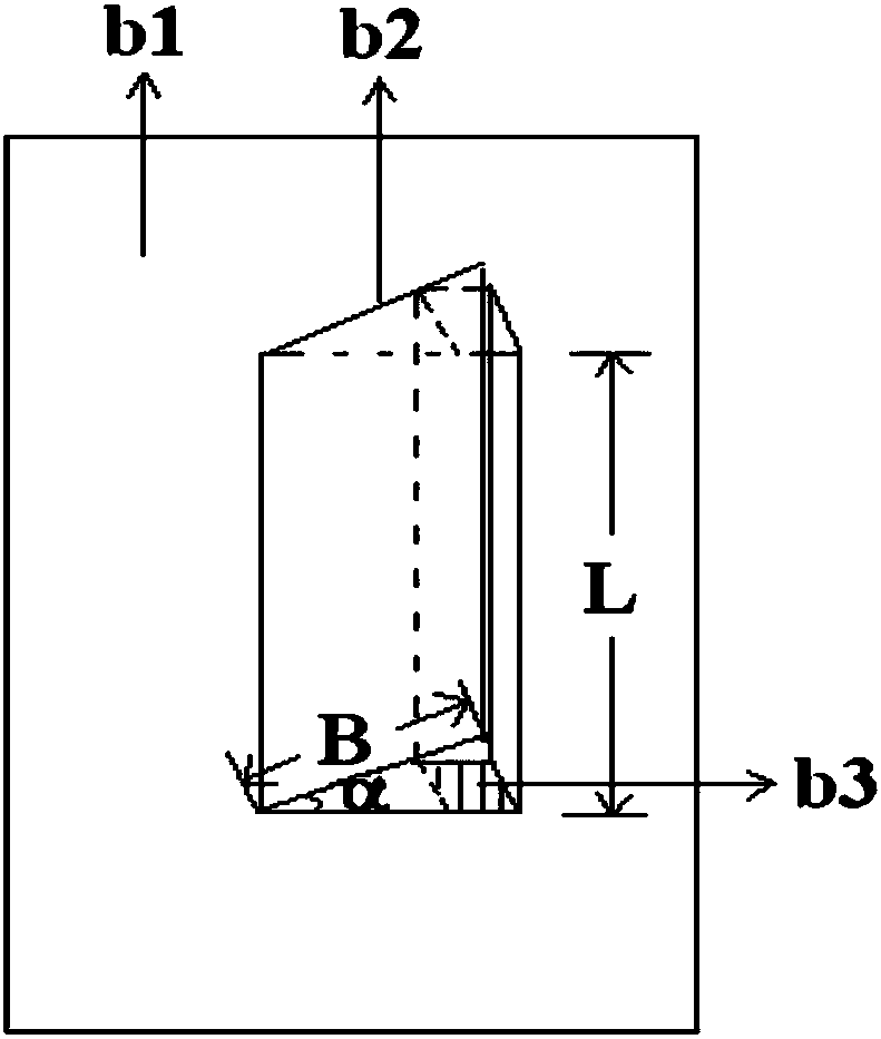
[0035] Firstly, a conventional hydrogen-hafnium co-doped indium oxide thin film a2 with a thickness of 80 nm was prepared on the doped layer on the light-facing surface of the crystalline silicon heterojunction solar cell a1 by radio frequency magnetron sputtering deposition method, and the deposition rate was The sputtering pressure is 1.2Pa. The substrate support b1 is parallel to the sputtering target surface, the substrate b2 is close to the substrate support b1, and the distance between the substrate support b1 and the target surface is 5.5 cm.

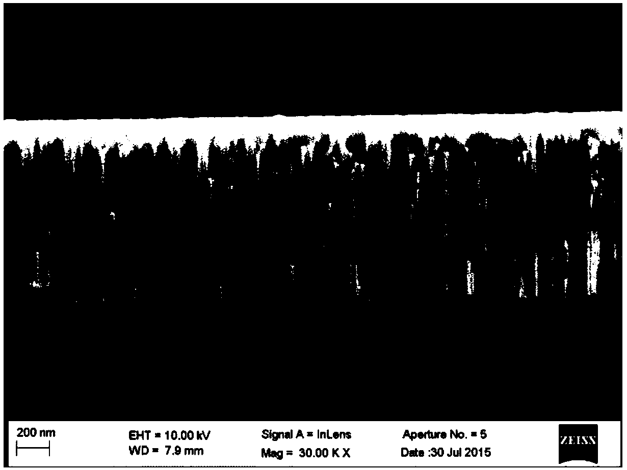
[0036] A layer of nano-column hydrogen hafnium co-doped indium oxide film a3 with a thickness of 20 nm was prepared on the conventional hydrogen-hafnium co-doped indium oxide film by radio frequency magnetron sputtering, and the deposit...

Embodiment 2

[0039] A high-purity indium oxide ceramic target with a hafnium dioxide doping amount of 0.5wt.% is used, the substrate temperature is 150°C, and the hydrogen partial pressure is 2×10 -2 Pa.

[0040] A layer of conventional hydrogen-hafnium co-doped indium oxide film a2 with a thickness of 70 nm was prepared on the surface of the doped layer on the light-facing side of the crystalline silicon heterojunction solar cell a1 by radio frequency magnetron sputtering deposition method, and the deposition rate was The sputtering pressure is 0.8Pa, the substrate support b1 is parallel to the sputtering target surface, the substrate b2 is closely attached to the substrate support b1, and the distance between the substrate support b1 and the target surface is 6cm. The refractive index of conventional hydrogen-hafnium co-doped indium oxide film prepared under this process condition is 2.1.

[0041] A layer of nano-column hydrogen hafnium co-doped indium oxide film a3 with a thickness of...

Embodiment 3

[0044] A high-purity indium oxide ceramic target with a hafnium dioxide doping amount of 2wt.% is used, the substrate temperature is 200°C, and the hydrogen partial pressure is 8×10 -2 Pa.

[0045] A conventional hydrogen-hafnium co-doped indium oxide thin film a2 with a thickness of 90 nm was first prepared on the doped layer of the crystalline silicon heterojunction solar cell a1 by radio frequency magnetron sputtering deposition method, and the deposition rate was The sputtering pressure is 1.5Pa, the substrate support b1 is parallel to the sputtering target surface, the substrate b2 is closely attached to the substrate support b1, and the distance between the substrate support b1 and the target surface is 4cm. The refractive index of conventional hydrogen-hafnium co-doped indium oxide film prepared under this process condition is 1.8.

[0046] On the conventional hydrogen-hafnium co-doped indium oxide film, a nano-column hydrogen-hafnium co-doped indium oxide film a3 wit...


PUM

PropertyMeasurementUnit
thicknessaaaaaaaaaa
thicknessaaaaaaaaaa
thicknessaaaaaaaaaa

Abstract

A composite conductive antireflective film for a crystalline silicon heterojunction solar cell comprises a conventional hydrogen hafnium co-doped indium oxide film having a refractive index of 1.8 to2.1 and a nano-column hydrogen hafnium co-doped indium oxide film having a refractive index of 1.4 to 1.6. The conventional hydrogen hafnium co-doped indium oxide film is deposited on the doped layerof the light-receiving surface of the solar cell. The nano-column hydrogen hafnium co-doped indium oxide film is deposited on the conventional hydrogen hafnium co-doped indium oxide film. The conventional hydrogen hafnium co-doped indium oxide film is RF magnetron sputtering deposited at a rate of 2 to 3 A / S. A substrate is parallel to the surface of a sputtering target material, and a film thickness is 70-90 nm. The nano-column hydrogen hafnium co-doped indium oxide film is RF magnetron sputtering deposited at rate of 0.5 to 1 A / S. A substrate has a certain angle to the surface of the sputtering target material, and a film thickness is 10-30 nm. The typical unheated composite conductive antireflective film has a resistivity of 4.3*10-4 [ohm]cm, a carrier concentration of 3.9*1020 cm-3, amobility of 56.5 cm2V-1s-1, and a weighted average reflectance of 3.53% in wavelength range of 500 to 1100 nm.. The composite film prepared by the invention functions as a cell conductive electrode and reduces light reflection.

Description

technical field [0001] The invention relates to a solar cell composite conductive anti-reflection film and a preparation method thereof. Background technique [0002] In order to improve the conversion efficiency of the solar cell, an optical anti-reflection film is usually required on the light-facing surface of the cell to ensure that as much light as possible is not reflected and enters the interior of the solar cell to be absorbed. For crystalline silicon heterojunction solar cells, transparent conductive oxide (TCO) acts as an electrode on the one hand, and on the other hand, it also plays a surface anti-reflection role similar to the silicon nitride layer on traditional crystalline silicon cells. [0003] If the nanostructure is made on the TCO anti-reflection layer on the surface of the battery, the anti-reflection effect can be greatly enhanced. In solar cells, TCO nano-films are mostly tin dioxide-doped indium oxide films, and their preparation methods include chem...

Claims


Application Information

Patent Timeline
Patent Type & Authority Applications(China)
IPC IPC(8): H01L31/0216H01L31/18
CPCH01L31/02168H01L31/1876Y02E10/50Y02P70/50
Inventor 王光红王文静赵雷刁宏伟
Owner INST OF ELECTRICAL ENG CHINESE ACAD OF SCI
Why Eureka
Try Eureka