Lamination package structure having pin side wall tin climbing function and manufacturing process thereof

A technology of packaging structure and manufacturing process, applied in semiconductor/solid-state device manufacturing, electrical components, electrical solid-state devices, etc., can solve problems such as delamination, increase joint area, save cutting costs, improve welding performance and welding reliability effect

Active Publication Date: 2018-06-22
JCET GROUP CO LTD
View PDF12 Cites 6 Cited by
  • Summary
  • Abstract
  • Description
  • Claims
  • Application Information

AI Technical Summary

Problems solved by technology

[0009] However, this kind of packaging structure that forms L-shaped outer leads or C-shaped outer leads by cutting ribs also has the following defects when forming L-shaped outer leads or C-shaped outer leads: first, when performing outer When the pins are formed, the outer pins are bent toward the side of the plastic package, Figure 1G and Figure

Method used


Image

  • Lamination package structure having pin side wall tin climbing function and manufacturing process thereof
  • Lamination package structure having pin side wall tin climbing function and manufacturing process thereof
  • Lamination package structure having pin side wall tin climbing function and manufacturing process thereof

Examples


Embodiment 1

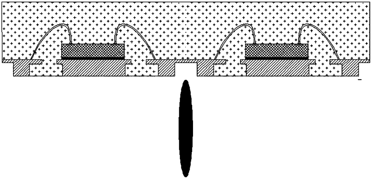
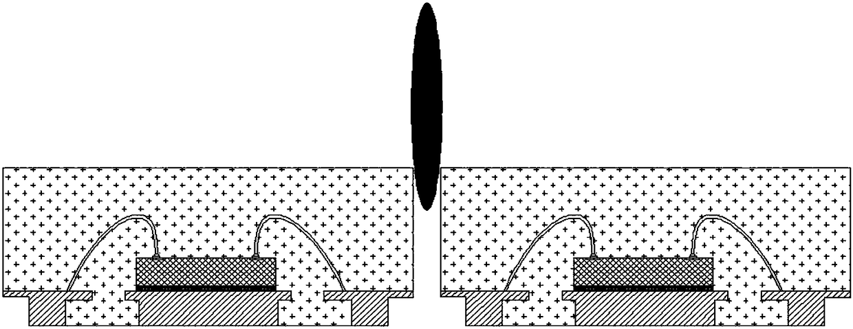
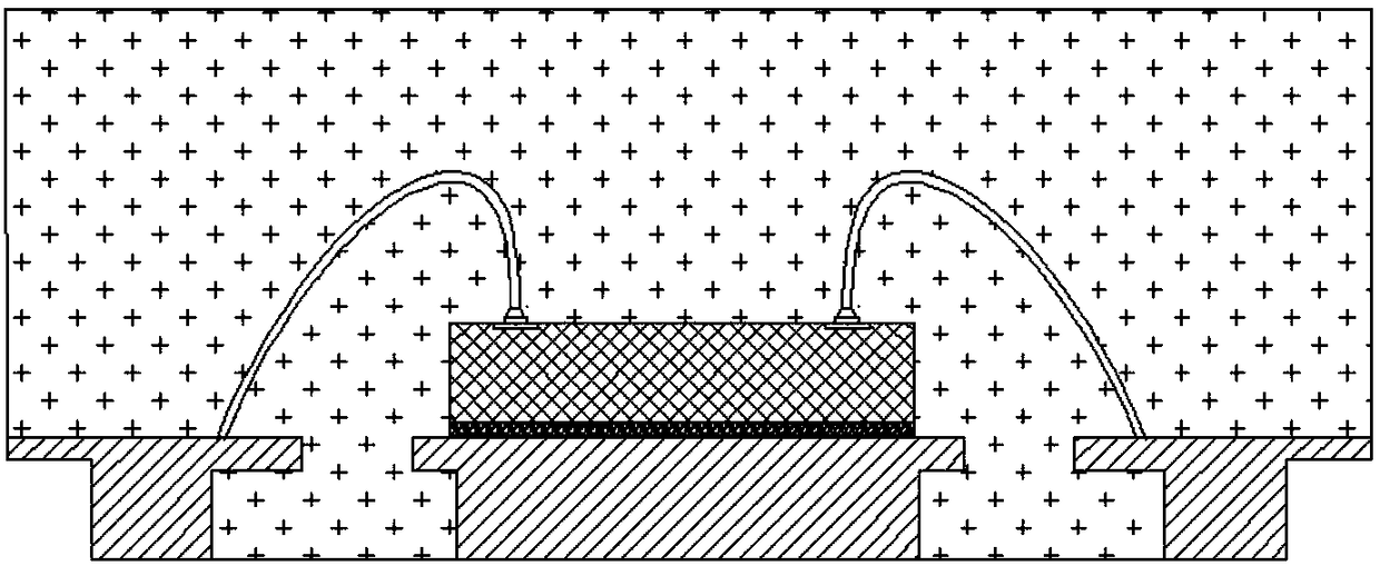
[0072] Such as figure 2 , image 3 As shown, in this embodiment, a package-on-package structure with the function of pin sidewall creeping tin, it includes a first base island 1 and a first pin 2, and the first base island 1 and the first pin 2 The metal wiring layer formed by electroplating, the first pin 2 is arranged around the first base island 1, the first pin 2 includes a plane part 2.1 and a side wall part 2.3, and the side wall part 2.3 is located on the plane part 2.1 Outer side, the side wall portion 2.3 includes multiple side wall surfaces, the plane portion 2.1 and the multiple side wall surfaces of the side wall portion 2.3 are transitionally connected by an arc portion 2.2, and the convex surface of the arc portion 2.2 faces outward On the lower side, the front of the first base island 1 is provided with a first chip 4 through an adhesive substance or solder 3, and the first chip 4 is electrically connected to the first pin 2 through a first metal bonding wire ...

Embodiment 2

[0086] see Figure 25 , the difference between embodiment 2 and embodiment 1 is that: the first chip and the second chip adopt a flip-chip structure;

Embodiment 3

[0088] see Figure 26 , the difference between embodiment 3 and embodiment 1 is that: the second chip adopts a flip-chip structure;


PUM


Abstract

The invention relates to a lamination package structure having a pin side wall tin climbing function and a manufacturing process thereof. The structure comprises a first paddle and a first pin, wherein the first pin comprises a planar part and a side wall part, the side wall part comprises a plurality of side wall surfaces, the planar part and the side wall part are in transition connection by anarc part, a first chip is arranged on a front surface of the first paddle, a first plastic sealing material wraps peripheral regions of the first paddle, the first pin and the first chip, a second paddle and a second pin are arranged on a surface of the first plastic sealing material, a second chip is arranged on a front surface of the second paddle, and a second plastic sealing material wraps peripheral regions of the second paddle, the second pin and the second chip. Welding tin can climb to a relatively high height along a vertical side wall during welding of a PCB, so that the bonding areaof the welding tin and the pins is expanded; and meanwhile, air at the pins can be discharged along protruding arcs, so that the welding performance and the welding reliability of a product are improved.

Description

technical field [0001] The invention relates to a stacked packaging structure with the function of tin climbing on the side wall of pins and a manufacturing process thereof, belonging to the technical field of semiconductor packaging. Background technique [0002] With the development of modern technology, semiconductor packaging has been widely used. Its extensive applications in radar, remote control telemetry, aerospace, etc. put forward higher and higher requirements for its reliability. The failure caused by poor soldering of semiconductors has attracted more and more attention, because this failure is often fatal and irreversible. Therefore, it is very important to get a good soldering reliability in the semiconductor industry. The tin layer on the soldering surface of the semiconductor can make the soldering stronger, especially for automotive electronics. [0003] As we all know, QFN (Quad Flat No-lead Package, four-sided leadless flat package) and DFN (DuadFlat No...

Claims


Application Information

Patent Timeline
IPC IPC(8): H01L23/31H01L23/49H01L23/498H01L21/48H01L21/56
CPCH01L21/4853H01L21/4889H01L21/56H01L23/3185H01L23/49H01L23/49811H01L2224/16245H01L2224/48091H01L2224/48247H01L2224/73265H01L2224/97H01L2924/181H01L2924/00014H01L2924/00012
Inventor 刘恺梁志忠王亚琴
Owner JCET GROUP CO LTD
Why Eureka
Try Eureka