Array substrate and preparation method thereof
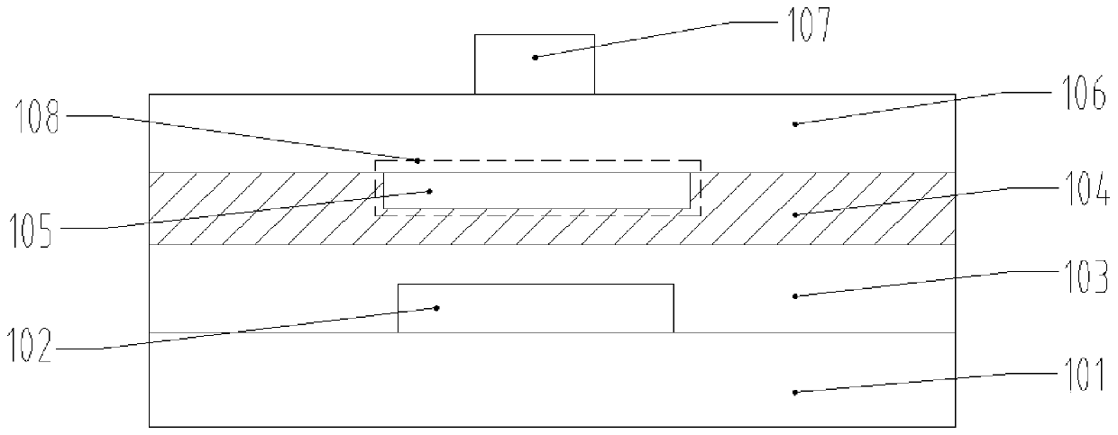
A technology for array substrates and base substrates, applied in the field of array substrates and their preparation, can solve problems affecting the electrical quality of panels, uneven film formation of gate insulating layers, and affecting normal display of panels, etc., to improve panel driving performance, improve Hump effect, the effect of improving uneven thickness
- Summary
- Abstract
- Description
- Claims
- Application Information
AI Technical Summary
Problems solved by technology
Method used
Image
Examples
preparation example Construction
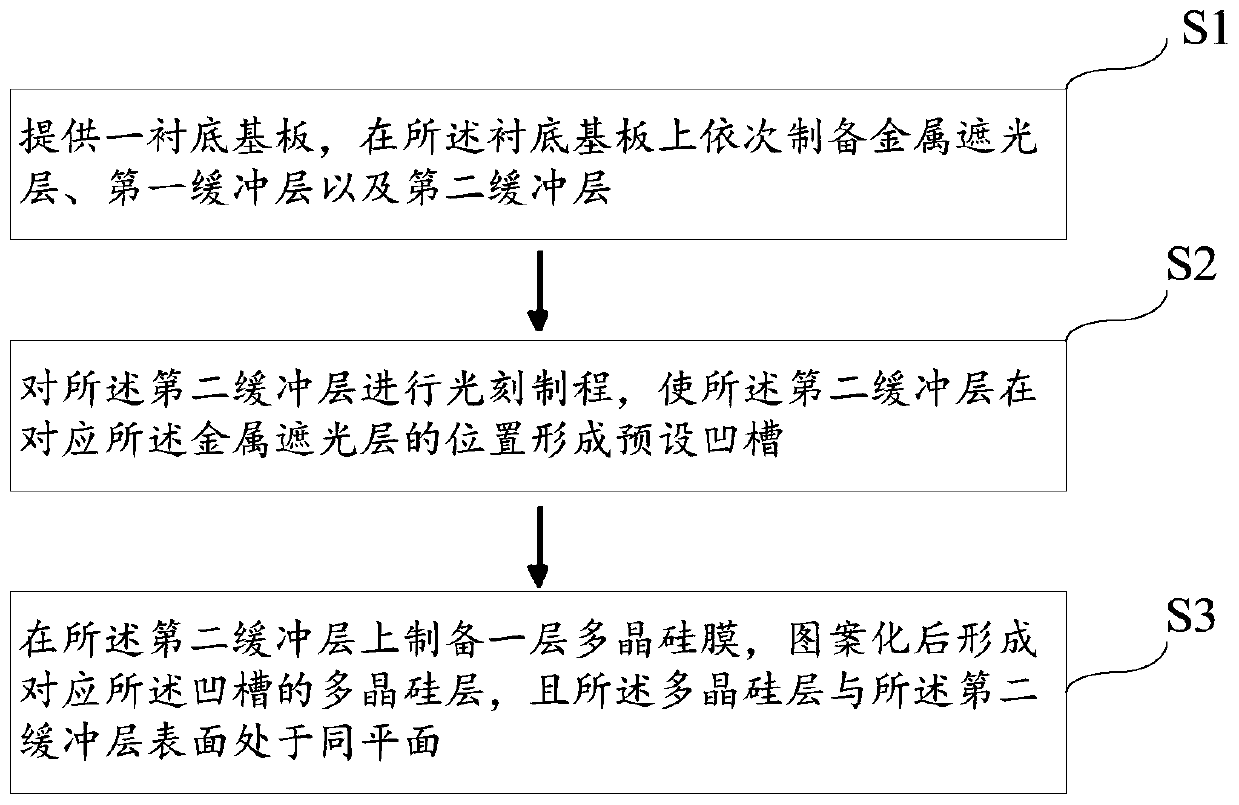
[0047] Such as figure 2 As shown, it is a flow chart of the preparation method of the array substrate provided by the embodiment of the present invention. The above preparation method of the array substrate includes the following steps:
[0048] Step S1: providing a base substrate, on which a metal light-shielding layer, a first buffer layer, and a second buffer layer are sequentially prepared;
[0049] Step S2: performing a photolithography process on the second buffer layer, so that the second buffer layer forms a predetermined groove at a position corresponding to the metal light-shielding layer;
[0050] Step S3: preparing a layer of polysilicon film on the second buffer layer, and forming a polysilicon layer corresponding to the groove after patterning, and the polysilicon layer is in the same plane as the surface of the second buffer layer.
[0051] Specifically, refer to Figures 3a-3d As shown in FIG. 1 , it is a schematic flow chart of the array substrate preparati...
Embodiment 2
[0056] Embodiment 2 provides another method for preparing the array substrate of the present invention. In this embodiment, a further improvement is made on the scheme of Embodiment 1, such as Figure 4 As shown, the method includes the following steps:
[0057] Step S101: providing a base substrate, on which a patterned metal light-shielding layer is prepared, and first coating a first buffer layer with the same thickness as the metal light-shielding layer on the base substrate;
[0058] Step S102: pattern the first buffer layer, etch the corresponding part of the first buffer layer corresponding to the metal light-shielding layer, so that the thickness of the patterned first buffer layer and the metal light-shielding layer are between same plane;
[0059] Step S103: coating the first buffer layer with a predetermined thickness on the patterned first buffer layer and the metal light-shielding layer;
[0060] Step S104: coating a second buffer layer on the first buffer layer...
PUM
 Abstract
Description
Claims
Application Information
 - R&D
- Intellectual Property
- Life Sciences
- Materials
- Tech Scout
- Unparalleled Data Quality
- Higher Quality Content
- 60% Fewer Hallucinations
Browse by: Latest US Patents, China's latest patents, Technical Efficacy Thesaurus, Application Domain, Technology Topic, Popular Technical Reports.
© 2025 PatSnap. All rights reserved.Legal|Privacy policy|Modern Slavery Act Transparency Statement|Sitemap|About US| Contact US: help@patsnap.com


