OLED encapsulation method and OLED encapsulation structure

A packaging method and packaging structure technology, which is applied in the manufacture of electrical components, electrical solid devices, semiconductor/solid devices, etc., can solve the problems of unfavorable curved screens, water and oxygen penetration, and small flexibility, so as to improve the packaging effect and good bending resistance The effect of improving the folding properties and improving the ability to block water and oxygen

Active Publication Date: 2018-06-22
WUHAN CHINA STAR OPTOELECTRONICS SEMICON DISPLAY TECH CO LTD
View PDF5 Cites 30 Cited by
  • Summary
  • Abstract
  • Description
  • Claims
  • Application Information

AI Technical Summary

Problems solved by technology

In addition, because the flexibility of the inorganic layer stacking region 3210 in the edge region 320 of the thin film encapsulation layer 300 is small, when the edge region 320 of the thin film encapsulation layer 300 is bent, the inorganic layer stacking region 3210 The barrier layer 500 is prone to breakage due to excessive stress, resulting in the infiltration of water and oxygen, which is not conducive to the realization of the currently popular curved screen (curved panel edge) design

Method used


Image

  • OLED encapsulation method and OLED encapsulation structure
  • OLED encapsulation method and OLED encapsulation structure
  • OLED encapsulation method and OLED encapsulation structure

Examples


Embodiment Construction

[0040] In order to further illustrate the technical means adopted by the present invention and its effects, the following describes in detail in conjunction with preferred embodiments of the present invention and accompanying drawings.

[0041] see figure 2 , the present invention provides a kind of OLED encapsulation method, comprises the following steps:

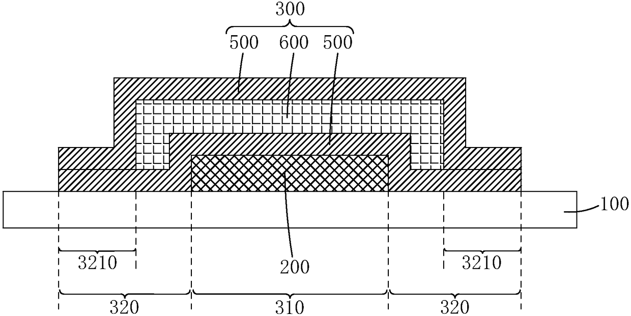
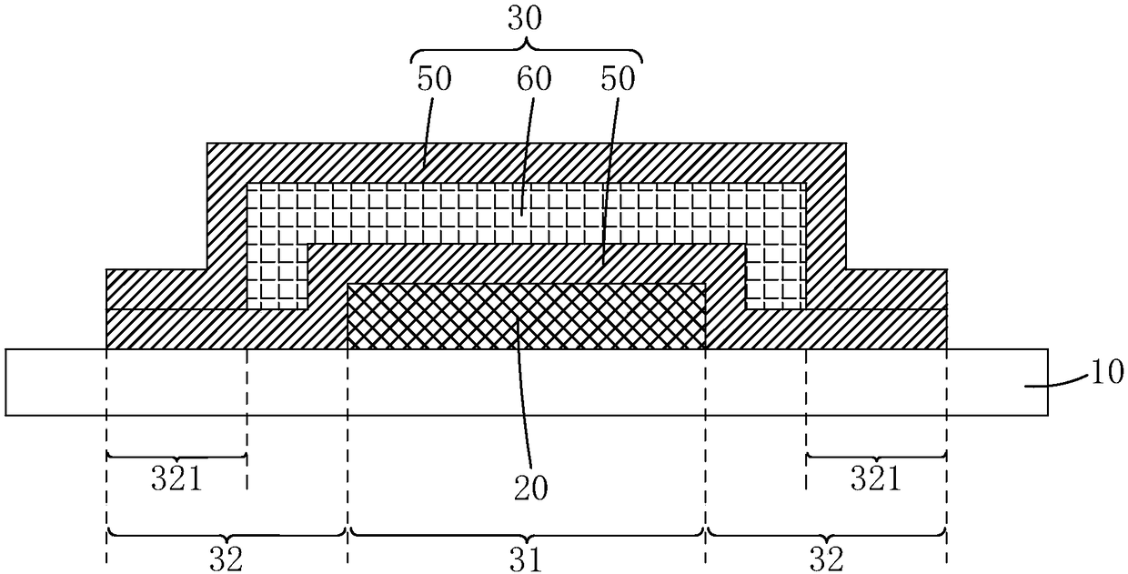
[0042] Step 1, such as image 3 and Figure 4 As shown, a base substrate 10 is provided, and an OLED device 20 is fabricated on the base substrate 10; a thin film encapsulation layer 30 covering the OLED device 20 is formed on the base substrate 10 and the OLED device 20;

[0043] In a direction parallel to the base substrate 10, the thin film encapsulation layer 30 includes a central region 31 corresponding to the top of the OLED device 20 and an edge region 32 corresponding to the periphery of the OLED device 20;

[0044] In the direction perpendicular to the base substrate 10, the thin film encapsulation layer 30 in...


PUM


Abstract

The invention provides an OLED encapsulation method and OLED encapsulation structure. The OLED encapsulation method includes the following steps: a first step, providing a substrate, and manufacturingan OLED device on the substrate, and forming a thin film encapsulation layer covering the OLED device on the substrate and the OLED device; and a second step, forming a circular organic layer distributed around the periphery of the thin film encapsulation layer on the thin film encapsulation layer and the substrate. The circular organic layer is arranged on the periphery of the thin film encapsulation layer, and in this way, a hook surface screen design and a narrow frame design of an OLED display device can be achieved, and the ability to block water and oxygen of the OLED encapsulation structure is improved. The OLED encapsulation structure can achieve the hook surface screen design and the narrow frame design of an OLED display device, and has high ability to block water and oxygen.

Description

technical field [0001] The invention relates to the field of display technology, in particular to an OLED packaging method and an OLED packaging structure. Background technique [0002] Organic Light Emitting Display (OLED) has many advantages such as self-luminescence, low driving voltage, high luminous efficiency, short response time, high definition and contrast, flexible display and large-area full-color display. It is recognized as the most promising display device in the industry. [0003] An OLED device generally includes: a substrate, an anode, a hole injection layer, a hole transport layer, a light-emitting layer, an electron transport layer, an electron injection layer, and a cathode. The light-emitting principle of OLED devices is that semiconductor materials and organic light-emitting materials are driven by an electric field to emit light through carrier injection and recombination. Specifically, OLED devices usually use indium tin oxide electrodes and metal e...

Claims


Application Information

Patent Timeline
Patent Type & Authority Applications(China)
IPC IPC(8): H01L51/52H01L51/56
CPCH10K50/844H10K50/8445H10K71/00H10K50/8426
Inventor 曾勉
Owner WUHAN CHINA STAR OPTOELECTRONICS SEMICON DISPLAY TECH CO LTD
Why Eureka
Try Eureka