Semiconductor device and formation method thereof

A technology for semiconductors and devices, applied in the field of semiconductor devices and their formation, can solve the problem that the electrical properties of semiconductor devices need to be improved, and achieve the effects of preventing oxidation, improving operating speed, and sufficient chemical reaction.

Inactive Publication Date: 2018-06-29
SEMICON MFG INT (SHANGHAI) CORP +1
View PDF4 Cites 3 Cited by
  • Summary
  • Abstract
  • Description
  • Claims
  • Application Information

AI Technical Summary

Problems solved by technology

[0004] However, the electrical performance of semiconductor devices formed by existing technologies still needs to be improved

Method used


Image

  • Semiconductor device and formation method thereof
  • Semiconductor device and formation method thereof
  • Semiconductor device and formation method thereof

Examples


Embodiment Construction

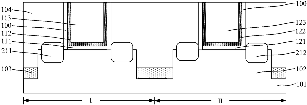
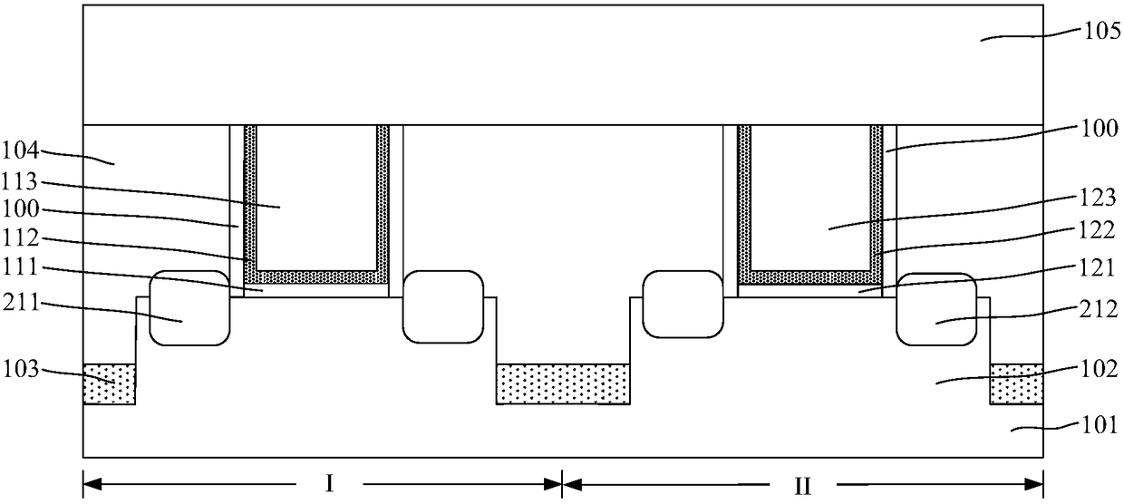
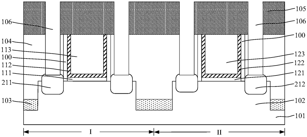
[0019] It can be seen from the background art that the electrical performance of semiconductor devices formed in the prior art needs to be improved.

[0020] In order to reduce the contact resistance of the source and drain of semiconductor devices, a metal silicide process has been proposed, among which, a post-metal silicide process (silicide last process) has been paid more and more attention. However, semiconductor devices formed by post-silicide processes have poor electrical performance.

[0021] It is found through analysis that the main reason for the poor electrical performance of the semiconductor device includes: the poor quality of the metal silicide layer formed on the source-drain doped region.

[0022] Further studies have found that in the process steps of forming the semiconductor device using a post-metal silicide process, in order to reduce the Schottky barrier height (SBH, Schottky Barrier Height) between the formed metal silicide and the source-drain doped...


PUM


Abstract

The invention relates to a semiconductor device and a formation method thereof. The formation method comprises that pre-non-crystallization processing is carried out on a source-drain doped region exposed out of the bottom of a first through hole; after pre-non-crystallization processing, a protection layer is formed on the source-drain doped region exposed out of the bottom of the first through hole; a pattern layer filling the first through hole is formed on the protection layer, and the pattern layer positioned in the top of a dielectric layer includes an opening; the dielectric layer is etched along the opening till the top of a gate structure is exposed, and a second through hole out of which the top of the gate structure is exposed is formed in the dielectric layer; the pattern layeris removed in the oxygen-containing atmosphere; the protection layer is removed; a metal contact layer is formed on the source-drain doped region exposed out of the bottom of the first through hole;and a conductive plug filling the first through hole is formed on the metal contact layer, and a gate plug filling the second through hole is formed at the same time. The contact resistance between the source-drain doped region and the metal contact layer is reduced, and the electrical performance of the semiconductor device is improved.

Description

technical field [0001] The invention relates to the technical field of semiconductor manufacturing, in particular to a semiconductor device and a forming method thereof. Background technique [0002] As the integration of semiconductor devices continues to increase, the critical dimensions of semiconductor devices continue to decrease, and correspondingly many problems have arisen, such as the corresponding increase in the surface resistance and contact resistance of the device's drain-source region, resulting in a decrease in the response speed of the device and signal occurrence. Delay. Therefore, an interconnection structure with low resistivity becomes a key element in the manufacture of highly integrated semiconductor devices. [0003] In order to reduce the contact resistance of the drain-source doped region of the device, a metal contact layer is formed on the source-drain doped region, and the material of the metal contact layer is metal silicide. The metal silicid...

Claims


Application Information

Patent Timeline
Patent Type & Authority Applications(China)
IPC IPC(8): H01L27/088H01L27/092H01L29/78H01L21/336
CPCH01L27/088H01L27/0886H01L27/092H01L27/0924H01L29/665H01L29/66795H01L29/785H01L2029/7858
Inventor 李勇
Owner SEMICON MFG INT (SHANGHAI) CORP
Why Eureka
Try Eureka