Niobium oxide gating appliance based on zirconia tunneling layer and its manufacturing method
A gating device and niobium oxide technology, applied in the field of information storage, can solve the problems of inability to meet the requirements of ultra-large-scale storage integration, low nonlinear ratio of the gating tube, etc., and achieve a safe and reliable cmos process, simple process, and good cycle tolerance. sexual effect
- Summary
- Abstract
- Description
- Claims
- Application Information
AI Technical Summary
Problems solved by technology
Method used
Image
Examples
Embodiment 1
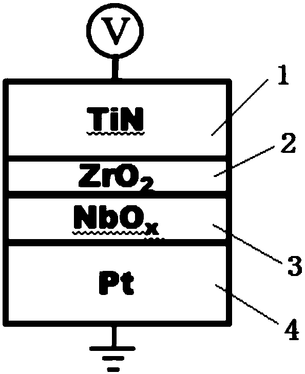
[0032] A niobium oxide gating device based on a zirconia tunneling layer in this embodiment, the device includes a bottom electrode layer 1, a tunneling layer 2, a conversion layer 3 and a top electrode layer 4 in sequence from bottom to top, wherein the The bottom electrode layer is made of TiN material, and the tunneling layer is made of zirconia (ZrO 2 ) thin film material, the conversion layer is a niobium oxide thin film material, and the top electrode layer is a Pt thin film material; the thickness of the bottom electrode layer is 200nm, the thickness of the tunneling layer is 3nm, and the thickness of the conversion layer The thickness of the top electrode layer is 45nm, and the thickness of the top electrode layer is 200nm; the shapes of the bottom electrode layer, the tunneling layer, the conversion layer and the top electrode layer are all square, and the side length of the square is 0.8 μm, and the unit structure of the gate device Schematic such as figure 1 shown....
Embodiment 2
[0044] A niobium oxide gating device based on a zirconia tunneling layer in this embodiment, the device includes a bottom electrode layer, a tunneling layer, a conversion layer and a top electrode layer in sequence from bottom to top, wherein the bottom electrode layer is TiN material, the tunneling layer is zirconia (ZrO 2 ) thin film material, the conversion layer is a niobium oxide thin film material, and the top electrode layer is a Pt thin film material; the thickness of the bottom electrode layer is 200nm, the thickness of the tunneling layer is 3nm, and the thickness of the conversion layer The thickness of the top electrode layer is 45nm, and the thickness of the top electrode layer is 200nm; the shapes of the bottom electrode layer, the tunneling layer, the conversion layer and the top electrode layer are all square, and the side length of the square is 1 μm.
[0045] The niobium oxide gating device based on the zirconia tunneling layer described above in this embodim...
Embodiment 3
[0056] A niobium oxide gating device based on a zirconia tunneling layer in this embodiment, the device includes a bottom electrode layer, a tunneling layer, a conversion layer and a top electrode layer in sequence from bottom to top, wherein the bottom electrode layer is FTO material, the tunneling layer is zirconia (ZrO 2 ) thin film material, the conversion layer is a niobium oxide thin film material, and the top electrode layer is a Pt thin film material; the thickness of the bottom electrode layer is 50nm, the thickness of the tunneling layer is 1nm, and the thickness of the conversion layer The thickness of the top electrode layer is 50nm; the shape of the bottom electrode layer, the tunneling layer, the conversion layer and the top electrode layer are all square, and the side length of the square is 100nm.
[0057] The niobium oxide gating device based on the zirconia tunneling layer described above in this embodiment is prepared according to the following method, and t...
PUM
| Property | Measurement | Unit |
|---|---|---|
| thickness | aaaaa | aaaaa |
| thickness | aaaaa | aaaaa |
| thickness | aaaaa | aaaaa |
Abstract
Description
Claims
Application Information


