AlN film preparation method based on patterned sapphire substrate and pre-sputtering technology

A technology for patterning sapphire and sapphire substrates, applied in semiconductor devices, electrical components, circuits, etc., can solve problems such as high threading dislocation density, lattice mismatch, and limited luminous efficiency improvement of AlN templates

Inactive Publication Date: 2018-07-10
PEKING UNIV
View PDF3 Cites 20 Cited by
  • Summary
  • Abstract
  • Description
  • Claims
  • Application Information

AI Technical Summary

Problems solved by technology

[0003] However, due to lattice mismatch and thermal mismatch, such AlN templates often have a high threading dislocation density (10 9 -10 10 cm -2 )
These threading dislocations generally extend into the active region of the de

Method used


Image

  • AlN film preparation method based on patterned sapphire substrate and pre-sputtering technology
  • AlN film preparation method based on patterned sapphire substrate and pre-sputtering technology
  • AlN film preparation method based on patterned sapphire substrate and pre-sputtering technology

Examples


Embodiment 1

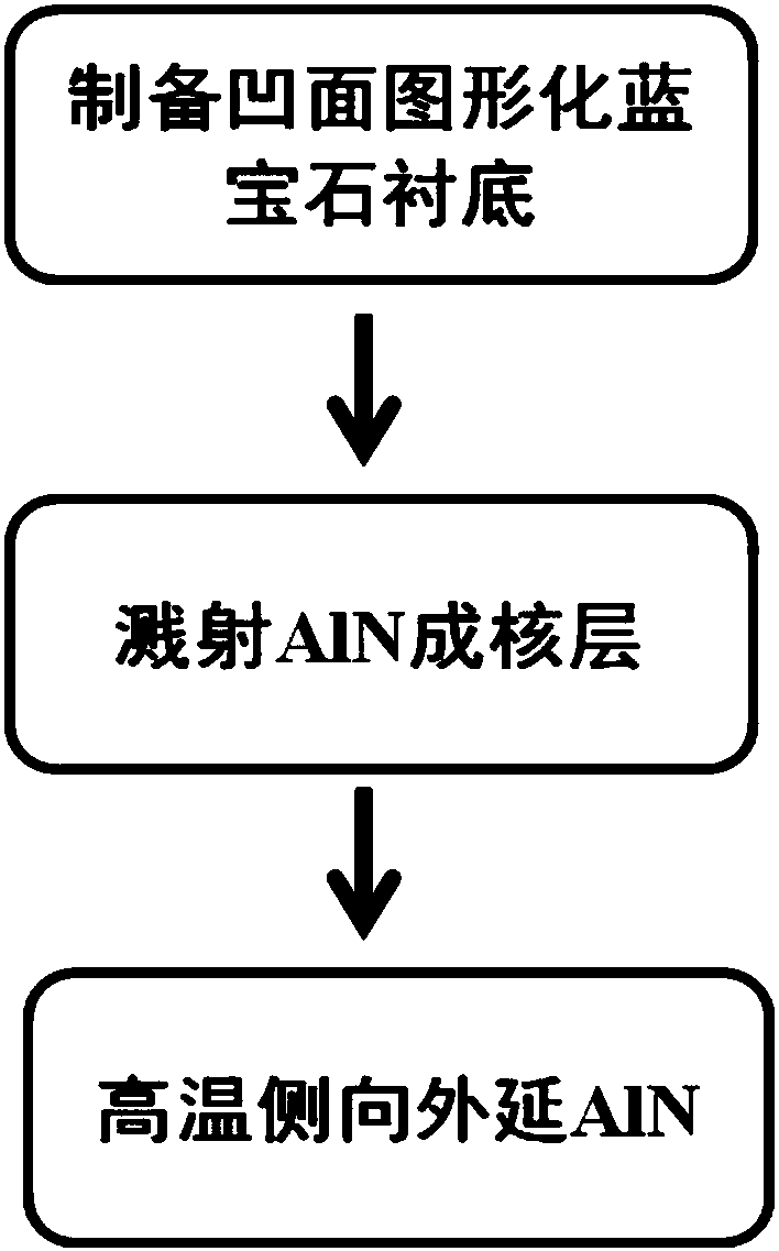
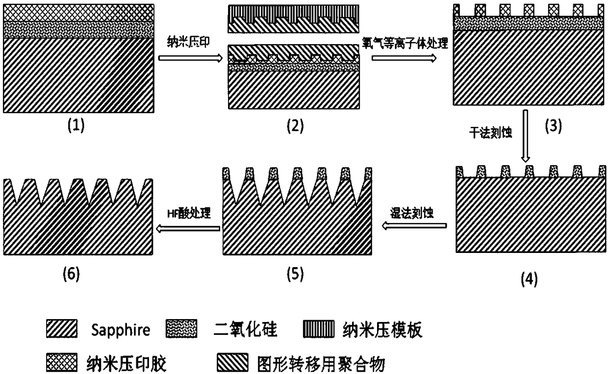
[0074] Example 1 (taking the preparation of a 5 micron AlN template as an example)

[0075] S1: Prepare a concave patterned sapphire substrate, the specific steps are:

[0076] 1) First use PECVD to deposit SiO with a thickness of 200nm on a 2-inch c-plane single-polished sapphire substrate 2 , and then spin coat TU7-220 glue with a thickness of 300nm.

[0077] 2) Using a nano imprinter The pattern transfer polymer on the embossing template (the mesa size is 350nm) with a period of 1 micron and a circular hole diameter of 650nm is placed on the polymer, and then the pattern on the polymer is embossed on the embossing glue under the condition of ultraviolet exposure.

[0078] 3) Using ICP to transfer the pattern to SiO with imprinting glue as a mask 2 superior.

[0079] 4) with SiO 2 Use H as a mask 2 SO 4 and H 3 PO 4 The mixed solution corrodes the sapphire at a temperature of 270°C, and transfers the pattern to the sapphire substrate.

[0080] 5) The remaining SiO...


PUM

PropertyMeasurementUnit
Thicknessaaaaaaaaaa

Abstract

The invention belongs to the field of III-family nitride semiconductor preparation technology, and relates to preparation of a low-dislocation-density AlN epitaxial film. The method of the invention is combined with two core key links of a patterned sapphire substrate and a pre-sputtering AlN nucleation layer. Based on the two core key links, a lateral epitaxial process is realized through metal organic chemical vapor deposition (MOCVD), thereby obtaining the AlN film with smooth surface and low dislocation density.

Description

technical field [0001] The invention relates to the technical field of quality control of Group III nitride semiconductor crystals, in particular to the preparation of low dislocation density AlN epitaxial films based on patterned sapphire substrate and pre-sputtering AlN nucleation layer technology. Background technique [0002] At present, there are two main technical routes for preparing AlN thin films in the world: the method of adjusting process parameters through low-temperature nucleation and high-temperature epitaxy on a flat sapphire substrate, or the method of micro-patterning sapphire substrate combined with MOCVD. Achieving reduced dislocations. [0003] However, due to lattice mismatch and thermal mismatch, such AlN templates often have a high threading dislocation density (10 9 -10 10 cm -2 ). These threading dislocations generally extend into the active region of the device, seriously affecting the performance of the device. Taking DUV light-emitting diod...

Claims


Application Information

Patent Timeline
IPC IPC(8): H01L33/00
CPCH01L33/007
Inventor 许福军沈波张立胜王明星解楠孙元浩秦志新
Owner PEKING UNIV
Why Eureka
Try Eureka