Micro light emitting diode wafer

A technology of light-emitting diodes and chips, which is applied in the direction of electrical components, circuits, semiconductor devices, etc., can solve problems such as difficulty in manufacturing, limitations, and unsuitability for miniature light-emitting diode chips, and achieve the effect of reducing the production process

Inactive Publication Date: 2018-07-17
PLAYNITRIDE
View PDF5 Cites 8 Cited by
  • Summary
  • Abstract
  • Description
  • Claims
  • Application Information

AI Technical Summary

Problems solved by technology

However, the method of making the above-mentioned multiple holes is generally suitable for larger-sized LED chips, but not suitable for small-sized miniature LED chips.
The reason is that the holes corresponding to the small-sized micro-LED chips are relatively small, so very precise alignment and hole-digging related manufacturing processes are required, so that the micro-LED chips have limitations in their manufacturing process and are not easy to manufacture.

Method used


Image

  • Micro light emitting diode wafer
  • Micro light emitting diode wafer
  • Micro light emitting diode wafer

Examples


Embodiment Construction

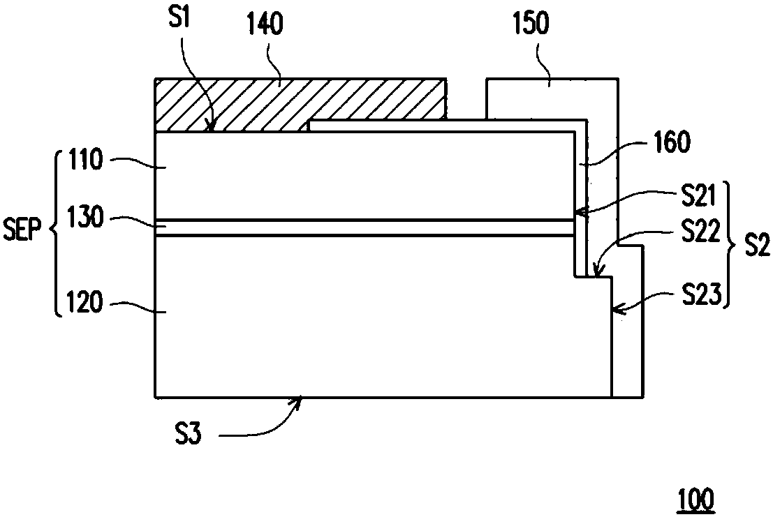
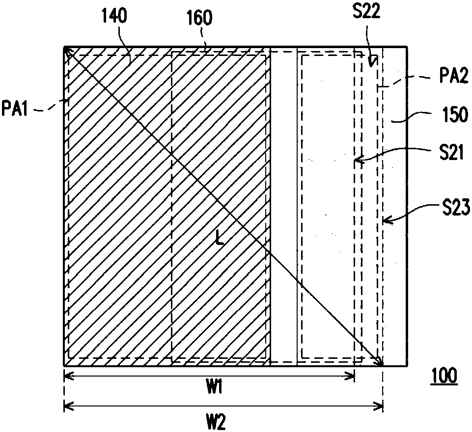
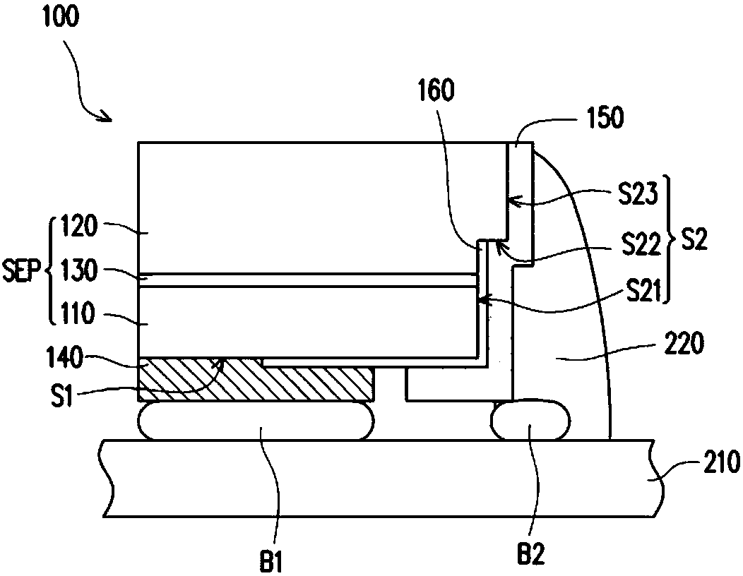
[0048] Figure 1A A cross-sectional schematic diagram showing a micro light emitting diode chip according to an embodiment of the present invention, please refer to Figure 1A . In this embodiment, the Micro Light-Emitting Diode (μLED) chip 100 includes an epitaxial structure SEP, an insulating layer 160, a first electrode 140 and a second electrode 150. Specifically, the epitaxial structure SEP has a first type doped semiconductor layer 110, a second type doped semiconductor layer 120, and a light emitting layer 130, and the light emitting layer 130 is located between the first type doped semiconductor layer 110 and the second type doped semiconductor layer 110. Between the semiconductor layers 120. The material of the semiconductor epitaxial structure SEP may be, for example, gallium nitride (GaN), indium gallium nitride (InGaN) or other semiconductor materials suitable for electroluminescence. The present invention does not limit the material of the semiconductor epitaxial str...


PUM


Abstract

The invention provides a micro light emitting diode wafer. The micro light emitting diode wafer comprises an epitaxy structure, a first electrode and a second electrode, wherein the epitaxy structurehas a first type doped semiconductor layer, a light emitting layer and a second type doped semiconductor layer and further comprises an upper surface and a side surface connected with the upper surface, the first electrode is arranged on the upper surface and is electrically connected with the first type doped semiconductor layer to provide first type carriers to enter the epitaxial structure fromat least a portion of the upper surface, the second electrode is arranged at the side surface and is electrically connected with the second type doped semiconductor layer to provide second type carriers to enter the epitaxial structure from at least a portion of the side surface, and the diagonal length of the micro light emitting diode wafer is greater than 0 and smaller than or equal to 140 microns. The micro light emitting diode wafer is advantaged in that the micro light emitting diode wafer is relatively easy to manufacture, and the light emitting area is relatively large.

Description

Technical field [0001] The invention relates to a light emitting diode chip, and particularly to a miniature light emitting diode chip. Background technique [0002] With the advancement of optoelectronic technology, the volume of many optoelectronic components is gradually becoming smaller. In recent years, due to breakthroughs in the size of light-emitting diodes (Light-Emitting Diodes, LEDs), micro-LED (micro-LED) displays made of light-emitting diodes arranged in arrays have gradually gained attention in the market. Miniature LED displays are active light-emitting element displays. In addition to being more power efficient compared to Organic Light-Emitting Diode (OLED) displays, they also have better contrast performance and can be exposed to sunlight. Visibility. In addition, since the micro light emitting diode display uses inorganic materials, it has better reliability and longer service life than organic light emitting diode displays. [0003] In the general horizontal ...

Claims


Application Information

Patent Timeline
Patent Type & Authority Applications(China)
IPC IPC(8): H01L33/38
CPCH01L33/385
Inventor 赖育弘罗玉云林子旸
Owner PLAYNITRIDE
Why Eureka
Try Eureka