High damage threshold liquid crystal binary optical panel with arbitrary amplitude shaping and its preparation method

A high damage threshold, binary optics technology, applied in optics, nonlinear optics, instruments, etc., can solve the problems of low damage threshold, high price, long processing cycle, etc., and achieve high aperture ratio, high damage threshold, damage threshold low effect

Active Publication Date: 2020-11-10
SHANGHAI INST OF OPTICS & FINE MECHANICS CHINESE ACAD OF SCI
View PDF5 Cites 0 Cited by
  • Summary
  • Abstract
  • Description
  • Claims
  • Application Information

AI Technical Summary

Problems solved by technology

The damage threshold of the dielectric film binary optical panel is high, but the processing cycle is long and the price is relatively expensive
In addition, active shaping devices such as electrical addressing and optical addressing liquid crystal light valves also have the disadvantage of low damage threshold due to the use of transparent conductive films.

Method used


Image

  • High damage threshold liquid crystal binary optical panel with arbitrary amplitude shaping and its preparation method
  • High damage threshold liquid crystal binary optical panel with arbitrary amplitude shaping and its preparation method
  • High damage threshold liquid crystal binary optical panel with arbitrary amplitude shaping and its preparation method

Examples


Embodiment Construction

[0038] The present invention will be described in detail below in conjunction with the accompanying drawings and specific embodiments. This embodiment is carried out on the premise of the technical solution of the present invention, and detailed implementation and specific operation process are given, but the protection scope of the present invention is not limited to the following embodiments.

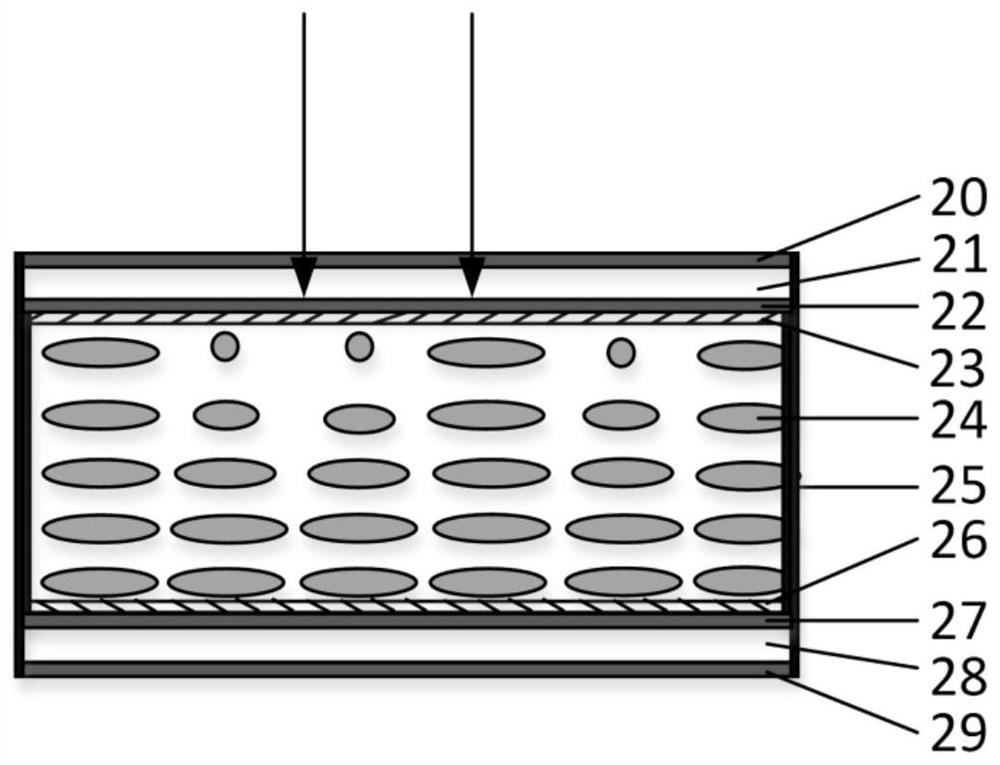
[0039] An arbitrary amplitude-shaping high damage threshold liquid crystal binary optical panel for arbitrary amplitude shaping of spatial light beams. The liquid crystal binary optical panel 2 is composed of a first dielectric film layer 20, a first glass substrate 21, a first chemical film layer 22, a photo-alignment film layer 23, a liquid crystal layer 24, a spacer frame 25, a rubbed alignment film layer 26, a second Chemical film layer 27, the second glass substrate 28 and the second dielectric film layer 29 constitute, and its film layer structure is as figure 1 shown;

[0040...


PUM

PropertyMeasurementUnit
optical damage thresholdaaaaaaaaaa

Abstract

The invention relates to an arbitrary amplitude shaping high damage threshold liquid crystal binary optical panel and a preparation method thereof. The arbitrary amplitude shaping high damage threshold liquid crystal binary optical panel comprises a first dielectric film layer, a first glass substrate, a first chemical film layer, an optical orientation film layer, a liquid crystal layer, a friction orientation film layer, a second chemical film layer, a second glass substrate, a second dielectric film layer and an interval sub frame. According to the panel, arbitrary amplitude shaping binarycoding figure is generated by a silicon substrate photo-etching system which comprises an LED (light-emitting diode) blue light source, an array lens, a collimator, a polarization beam splitter, a silicon substrate liquid crystal space light modulator, an achromatic imaging system and a computer, and the figure is inscribed on the optical orientation film layer of the liquid crystal binary opticalpanel to obtain the arbitrary amplitude shaping high damage threshold liquid crystal binary optical panel. The arbitrary amplitude shaping high damage threshold liquid crystal binary optical panel has the advantages that the panel is rewritable, high in damage threshold and shaping accuracy and the like.

Description

technical field [0001] The invention belongs to laser beam spatial near-field shaping, in particular to a high damage threshold liquid crystal binary optical panel with arbitrary amplitude shaping. The invention is especially suitable for any amplitude type liquid crystal binary optical panel modulated by 1053nm linearly polarized light (but not limited to this wavelength) and its preparation method. Background technique [0002] In laser beam delivery systems, spatial near-field amplitude shaping of laser beams can be achieved by using binary optical panels or liquid crystal light valves. The binary optical panel converts the intensity transmittance into the density distribution of light transmission points, usually there are two types of chrome-plated binary optical panels and dielectric film binary optical panels. Chrome-plated binary optical panels are capable of high shaping accuracy but have a low damage threshold due to the utilization of chrome-mask technology. The...

Claims


Application Information

Patent Timeline
Patent Type & Authority Patents(China)
IPC IPC(8): G02F1/1333G02F1/1337
CPCG02F1/1333G02F1/133711
Inventor 范薇夏刚黄大杰程贺郭江涛
Owner SHANGHAI INST OF OPTICS & FINE MECHANICS CHINESE ACAD OF SCI
Why Eureka
Try Eureka