
Organic photoelectric detector responded by broadband spectrum

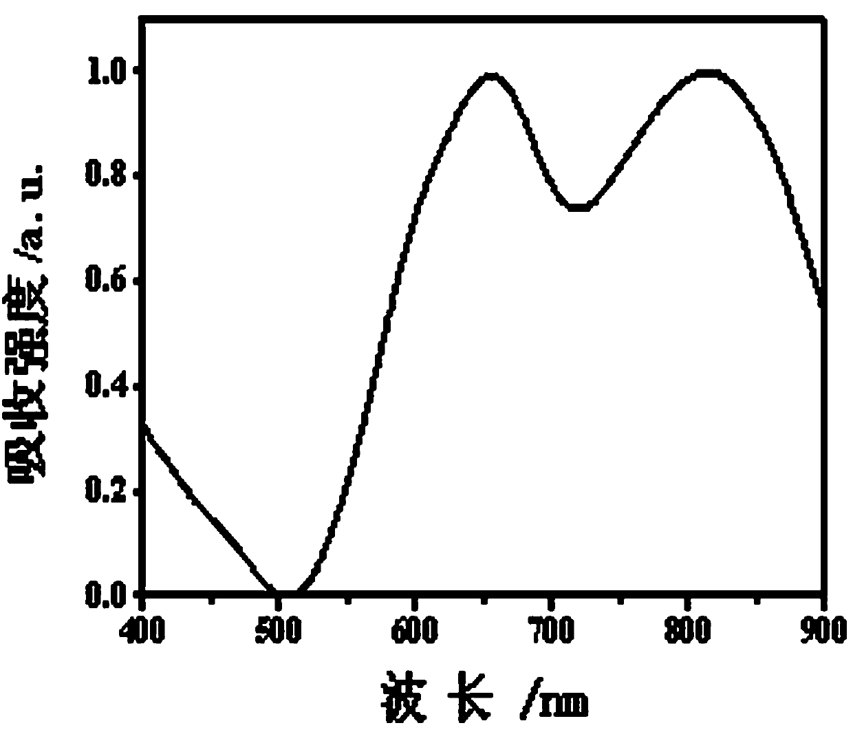
A photodetector and wide-spectrum technology, which is applied in the field of optoelectronics, can solve the problems of visible light and near-infrared light having no responsiveness, limitation, and inability to completely cover the visible light region, etc., and achieve high molar absorption coefficient, simple device structure and manufacturing process, Applying the effect of an area light

Active Publication Date: 2018-07-27
NANJING UNIV OF POSTS & TELECOMM
View PDF10 Cites 5 Cited by
  • Summary
  • Abstract
  • Description
  • Claims
  • Application Information

AI Technical Summary

Problems solved by technology

However, since the absorption edge of P3HT is around 650 nm and cannot completely cover the visible light region, the fabricated device has no responsiveness to visible light and near-infrared light beyond 650 nm.
This defect limits the utilization of the solar spectrum by P3HT:PCBM solar cells, and also limits the application of P3HT:PCBM photodetectors in broad spectral response and near-infrared detectors.

Method used


Image

  • Organic photoelectric detector responded by broadband spectrum
  • Organic photoelectric detector responded by broadband spectrum
  • Organic photoelectric detector responded by broadband spectrum

Examples


Embodiment Construction

[0019] In order to enable those skilled in the art to better understand the solutions of the present invention, the technical solutions in the embodiments of the present invention will be clearly and completely described below in conjunction with the drawings in the embodiments of the present invention. Apparently, the described embodiments are only a part of the embodiments of the present invention, rather than all the embodiments, and the preferred embodiments of the present invention are shown in the accompanying drawings. The present invention can be implemented in many different forms and is not limited to the embodiments described herein, on the contrary, these embodiments are provided for the purpose of making the disclosure of the present invention more thorough and comprehensive. Based on the embodiments of the present invention, all other embodiments obtained by persons of ordinary skill in the art without creative efforts fall within the protection scope of the prese...


PUM


Abstract

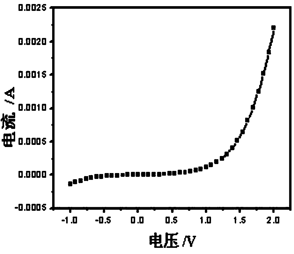
The invention discloses an organic photoelectric detector responded by a broadband spectrum. The detector comprises a substrate, a transparent conductive layer, an anode modifying layer, a photosensitive layer, a hole blocking layer and a cathode layer which are sequentially stacked, wherein the thickness of the transparent conductive layer is 100-150 nanometers, the thickness of the anode modifying layer is 35-50 nanometers, the thickness of the photosensitive layer is 100-240 nanometers, the thickness of the hole blocking layer is 35-50 nanometers, the thickness of the cathode layer is 80-120 nanometers, the transparent conductive layer is made of a conductive material, the anode modifying layer is made of a P-type semiconductor material, the photosensitive layer is made of a mixture containing an organic polymer donor material, a micromolecule donor material and an acceptor material, the hole blocking layer is made of an N-type semiconductor material, and the cathode layer is made of a low-work-content metal material; the device structure and manufacturing technology are simple, the light response range of the photosensitive layer is enlarged, the response degree of light signals to be detected can be remarkably increased, and the detector has the large advantage, is not sensitive to temperature, has multiple application scenes and is convenient to popularize.

Description

technical field [0001] The invention relates to the field of optoelectronics, in particular to an organic photodetector with wide spectral response. Background technique [0002] Photodetectors are devices that convert optical signals into electrical signals. According to their response wavelength range, they can be divided into wide spectral response photodetectors and narrow spectral response photodetectors. Among them, photodetectors with wide spectral response have important applications in many aspects such as image sensing, remote control, and day and night surveillance. Compared with inorganic photodetectors, organic photodetectors have the advantages of good flexibility, low manufacturing cost, and a wide range of material choices. However, the response range of organic photodetectors is usually limited to the near-ultraviolet to visible light bands. So far, they have high sensitivity to near-infrared light. There are not many reports on sensitive organic photodetec...

Claims


Application Information

Patent Timeline
Patent Type & Authority Applications(China)
IPC IPC(8): H01L51/42H01L51/46
CPCH10K85/1135H10K85/215H10K30/30Y02E10/549Y02P70/50
Inventor 杨天赦李向领赵强徐云剑刘淑娟黄维
Owner NANJING UNIV OF POSTS & TELECOMM
Learn More