Method for manufacturing CIGS thin-film solar cell by using dry buffer layer

A solar cell and buffer layer technology, applied in circuits, photovoltaic power generation, electrical components, etc., can solve the problems of poor continuity of CIGS thin-film solar cells and small band gap of the buffer layer, etc., to improve continuity, improve efficiency, increase Effect of Spectral Response Range

Inactive Publication Date: 2016-02-24
BEIJING SIFANG CRENERGEY OPTOELECTRONICS TECH CO LTD +1
View PDF3 Cites 8 Cited by
  • Summary
  • Abstract
  • Description
  • Claims
  • Application Information

AI Technical Summary

Problems solved by technology

[0004] The purpose of the present invention is aimed at (1) CdS buffer layer contains cadmium in the prior art; (2) because wet process exists, the continuity of CIGS thin-film solar cell preparation is bad; (3) buffer layer bandgap is less etc. three Aspects Proposed a new preparation method for CIGS thin film solar cell buffer layer

Method used


Image

  • Method for manufacturing CIGS thin-film solar cell by using dry buffer layer
  • Method for manufacturing CIGS thin-film solar cell by using dry buffer layer
  • Method for manufacturing CIGS thin-film solar cell by using dry buffer layer

Examples


Embodiment 1

[0036] The manufacturing method of the battery is as follows:

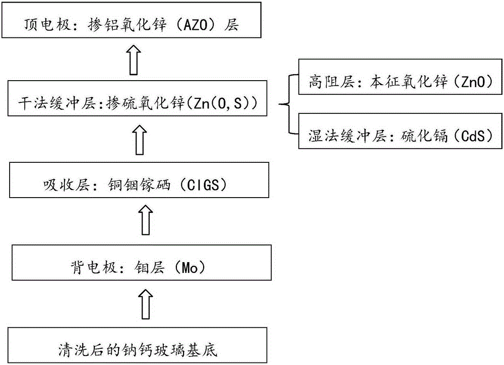
[0037] In step 1, a Mo layer is prepared on a soda-lime glass substrate, and the thickness of the film layer is 0.8 μm.

[0038] In step 2, a CIGS layer is prepared on the Mo layer, and the thickness of the film layer is 2 μm.

[0039] Step 3: Prepare a Zn(O,S) layer on the CIGS layer by DC magnetron sputtering, wherein the atomic ratio of O to S is 15%, and the power density is 1.56W / cm 2 , the background vacuum is 3×10 -3 Below Pa, the sputtering pressure is 1Pa, and the thickness of the film layer is 100nm.

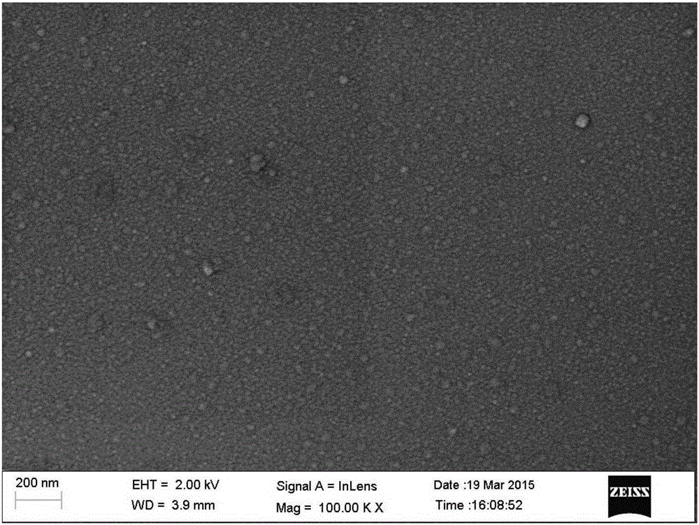
[0040] Step 4, the prepared Zn(O,S) thin film layer is annealed in the air at 150°C, and the attached image 3 And attached Figure 4 By comparison, it is found that the surface of the annealed film becomes smooth, and the average particle size does not change significantly. The annealing treatment makes the surface atoms migrate, thereby improving the surface roughness of the film.

[0041] Step five...

Embodiment 2

[0046] The third step above is to prepare a Zn(O,S) layer on the CIGS layer by using DC magnetron sputtering, wherein the atomic ratio of O to S is 30%, and the power density is 1.56W / cm 2 , the background vacuum is 3×10 -3 Below Pa, the sputtering pressure is 1Pa, and the thickness of the film layer is 100nm.

[0047] In the above step 4, the prepared Zn(O, S) thin film layer is annealed in air at 250°C, and the attached Figure 5 And attached Figure 6 By comparison, it is found that as the atomic ratio of O and S decreases, the surface roughness of the film decreases, and the surface of the film after annealing is smoother, with a significantly larger average particle size and better crystallinity.

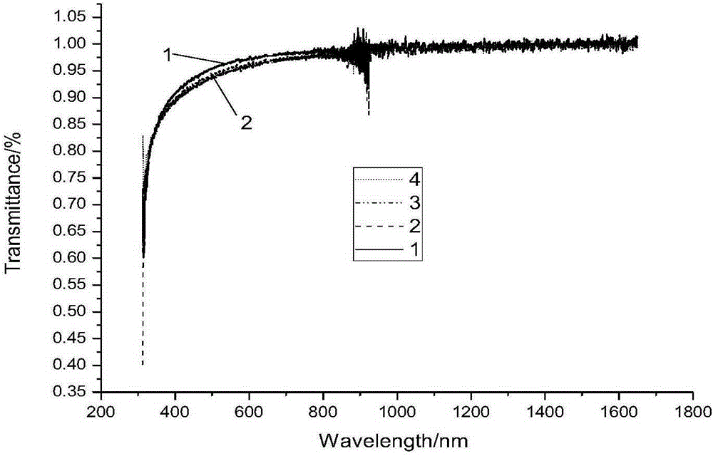
[0048] attached by figure 2 It can be seen that the transmittance of the Zn(O,S) film is higher than 90% in the range of 400-1800nm, and its band gap is 3.55eV, which is slightly lower than that of Example 1, and compared with the SLG prepared under the same conditions ( C...

Embodiment 3

[0052] The third step above is to prepare a Zn(O,S) layer on the CIGS layer by using DC magnetron sputtering, wherein the atomic ratio of O to S is 10%, and the power density is 2.33W / cm 2 , the background vacuum is 3×10 -3 Below Pa, the sputtering pressure is 1Pa, and the thickness of the film layer is 100nm.

[0053] In the above step 4, the prepared Zn(O, S) thin film layer is annealed in air at 150°C, and the attached figure 2 It can be seen that the transmittance of the Zn(O,S) film is higher than 90% in the range of 400-1800nm, but slightly lower than that of Example 1 and Example 2, and its band gap is 3.5eV, which is comparable to that of the SLG prepared under the same conditions. Compared with the (soda-lime glass) / Mo / CIGS / CdS / ZnO / AZO structure, the opening voltage can be increased by 3%-5%, the battery efficiency can be increased by 0.5%-2%, and the decrease in the band gap value is related to the decrease in the S ratio.


PUM

PropertyMeasurementUnit
thicknessaaaaaaaaaa
thicknessaaaaaaaaaa
thicknessaaaaaaaaaa

Abstract

The invention relates to a method for manufacturing a CIGS thin-film solar cell by using a dry buffer layer. The method comprises: step 1, preparing a Mo layer on a piece of soda-lime glass; step 2, preparing a CIGS layer on the Mo layer; step 3, preparing a Zn (O,S) thin film layer on the CIGS layer by using a direct-current magnetron sputtering method; step 4, carrying out annealing processing on the prepared Zn (O,S) thin film layer in air to release the stress, thereby improving the film quality; and step 5, preparing an AZO layer on the Zn (O,S) thin film layer to form a CIGS thin-film solar cell device. According to the invention, during the preparation process, no waste liquid is generated, so that no influence on the preparation staff and the environment is caused; and the continuity of the preparation process of the CIGS cell device is improved. Because of the dry buffer layer, absorption of the blue light can be reduced effectively, the response range of the spectrum can be enlarged, and the solar cell efficiency can be enhanced.

Description

technical field [0001] The invention belongs to the technical field of thin film solar cells, and in particular relates to a method for preparing a dry buffer layer of a copper indium gallium selenide (CIGS) thin film solar cell, and a structure based on the dry buffer layer applied to the CIGS thin film solar cell. Background technique [0002] Energy crisis and environmental pollution are two basic problems facing the world today. Cu(In,Ga)Se2(CIGS) thin film has high absorption coefficient for visible light, appropriate band gap, strong radiation resistance, stable battery performance, and good low-light performance. It is considered to be one of the most promising optoelectronic materials. [0003] The traditional CIGS thin film solar cell is SLG (soda lime glass) / Mo / CIGS / CdS / ZnO / AZO structure, in which the buffer layer is cadmium sulfide (CdS), its function is as follows: because CIGS thin film and zinc oxide (ZnO) exist Larger lattice mismatch, directly depositing ZnO...

Claims


Application Information

Patent Timeline
Patent Type & Authority Applications(China)
IPC IPC(8): H01L31/18
CPCH01L31/0322Y02E10/541Y02P70/50
Inventor 张宁余新平赵莉张亚飞陈玉峰李俊林
Owner BEIJING SIFANG CRENERGEY OPTOELECTRONICS TECH CO LTD
Why Eureka
Try Eureka