Multi-mode POR circuit for FPGA

A multi-mode and circuit technology, applied in the field of FPGA, can solve the problems that POR circuits cannot meet the delay requirements, and achieve the effects of simple design, flexible application, and reduced dynamic power consumption

Active Publication Date: 2018-07-31
XIAN INTELLIGENCE SILICON TECH INC
View PDF5 Cites 1 Cited by
  • Summary
  • Abstract
  • Description
  • Claims
  • Application Information

AI Technical Summary

Problems solved by technology

[0004] Existing POR circuits cannot meet the flexible delay requirements of FPGA complex work scenarios, so it is becoming more and more important to provide a multi-mode POR circuit that can meet the application requirements of FPGA complex work scenarios

Method used


Image

  • Multi-mode POR circuit for FPGA
  • Multi-mode POR circuit for FPGA
  • Multi-mode POR circuit for FPGA

Examples


Embodiment 1

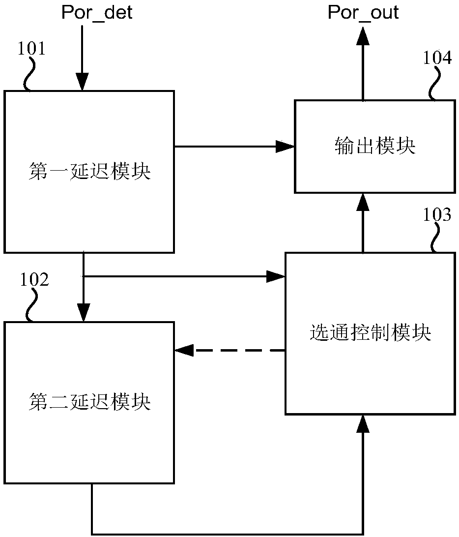
[0039] See figure 1 , figure 1 A schematic diagram of a multi-mode POR circuit for FPGA provided by an embodiment of the present invention, including: a first delay module 101, a second delay module 102, a gating control module 103 and an output module 104; wherein,

[0040] The first output end of the first delay module 101 is electrically connected to the second delay module 102 and the gating control module 103 respectively, and the second output end of the first delay module 101 is electrically connected to the output module 104 The second delay module 102 is electrically connected to the gating control module 103; the gating control module 103 is electrically connected to the output module 104.

[0041] Specifically, the delay length of the second delay module 102 is greater than the delay length of the first delay module 101 .

[0042] Preferably, the first delay module 101 is a microsecond-level delay circuit; the second delay module 102 is a millisecond-level D flip-...

Embodiment 2

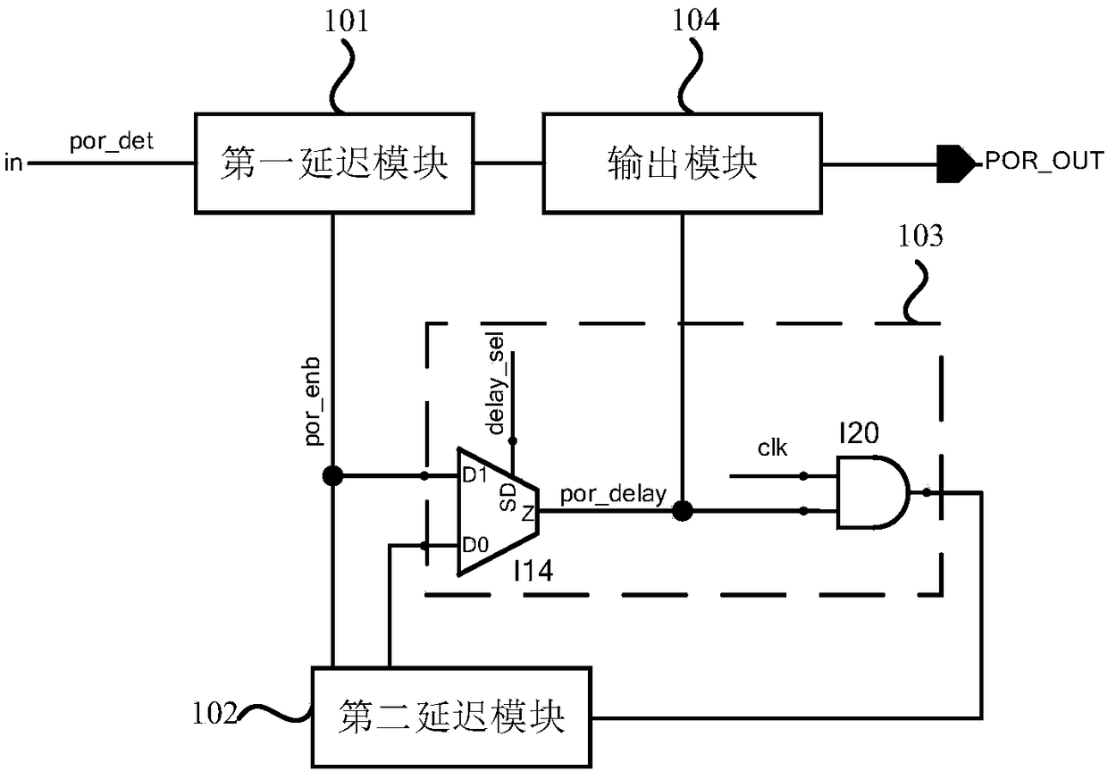
[0045] In order to facilitate the understanding of the working principle of the present invention, this embodiment describes in detail the optimized structure of the gating control module of the POR circuit on the basis of the above embodiments.

[0046] Specifically, see figure 2 , figure 2 A schematic diagram of a gating control module circuit structure provided by an embodiment of the present invention, the gating control module 103 may include a one-two selector I14; wherein, the first input terminal D1 of the one-two selector I14 is electrically Connect the first output terminal of the first delay module 101, the second input terminal D0 of the two-choice selector I14 is electrically connected to the output terminal of the second delay module 102; the two-choice selector I14 The output terminal Z is electrically connected to the output module 104 .

[0047] Further, the gate control module 103 also includes an AND gate I20; wherein, the first input end of the AND gate...

Embodiment 3

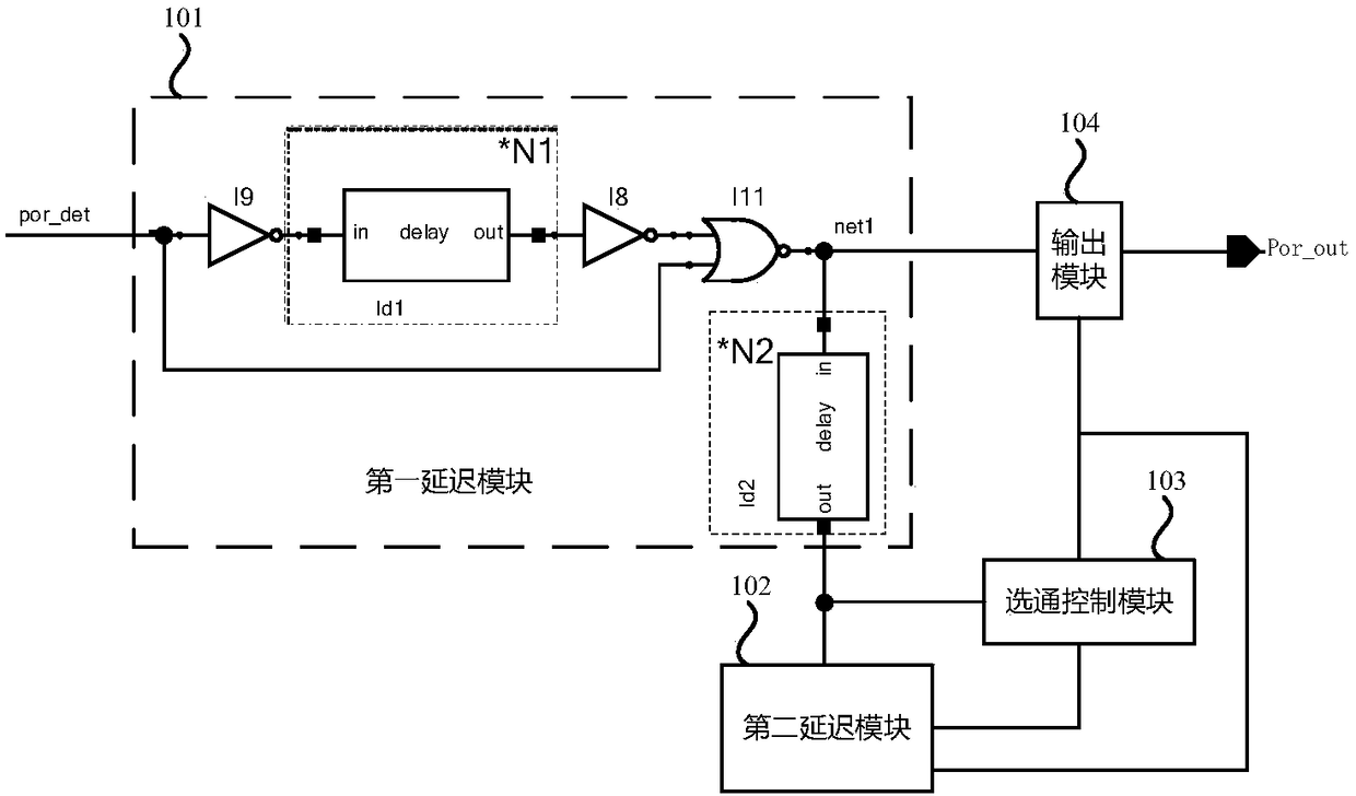
[0051] In order to facilitate the understanding of the working principle of the present invention, this embodiment describes in detail the optimized structure of the first delay module of the POR circuit on the basis of the above embodiments.

[0052] Specifically, see image 3 , image 3 The first delay module circuit structure schematic diagram provided for the embodiment of the present invention includes: a first inverter I9, a first delay unit Id1, a second inverter I8, a first NOR gate I11 and a second delay unit Id2; in,

[0053] The first inverter I9, the first delay unit Id1, and the second inverter I8 are sequentially connected in series to an input end of the first NOR gate I11, and the first NOR gate I11 The other input end of the first inverter I9 is ​​electrically connected to the input end of the multi-mode POR circuit, and the output end of the first NOR gate I11 is electrically connected to the second delay unit Id2 and the The output module 104; the second ...


PUM


Abstract

The present invention relates to a multi-mode POR circuit for an FPGA, comprising: a first delay module (101), a second delay module (102), a gating control module (103), and an output module (104), wherein a first output end of the first delay module (101) is electrically connected to the second delay module (102) and the gating control module (103) respectively, and a second output end of the first delay module (101) is electrically connected to the output module (104) is connected; the second delay module (102) is electrically connected to the gating control module (103); and the gating control module (103) is electrically connected to the output module (104). The multi-mode POR circuit provided by the invention can flexibly control the delay of a POR circuit from a subtle level to a few hundred milliseconds level; and meanwhile, the clock and reset of a D trigger are controlled by the output of a selector, the clk signal can be shielded according to needs in variosu modes, and theD trigger no longer acts, thereby reducing the dynamic power consumption of the circuit.

Description

technical field [0001] The invention belongs to the technical field of FPGA, and in particular relates to a multi-mode POR circuit for FPGA. Background technique [0002] Field-Programmable Gate Array (FPGA) is a logic device composed of many logic units, among which logic units include gates, look-up tables and flip-flops. It has rich hardware resources, powerful parallel processing capabilities and flexible The reconfigurable capability has been widely used in many fields such as data processing, communication, and network. [0003] The power-on reset (Power-on Reset, POR) circuit is a sub-module inside the integrated circuit (Integrated Circuit, IC), which is used to reset and clear the voltage of each node of the internal circuit when the internal digital circuit of the IC is powered on. Make the circuit work as designed. Due to the rich internal resources of the FPGA, different resources have different requirements for POR delay, which may range from microseconds to m...

Claims


Application Information

Patent Timeline
IPC IPC(8): H03K19/177
CPCH03K19/1774
Inventor 孟智凯冯晓玲贾红程显志陈维新韦嶔
Owner XIAN INTELLIGENCE SILICON TECH INC
Why Eureka
Try Eureka